Researchers improve silicon-based semiconductor technology by developing next-generation, 2D semiconductors that have the ability to power future AI systems.
To achieve Artificial Intelligence (AI) systems that have the potential to power autonomous driving, processors that function as the brain of computers must be able to process more data. However, silicon-based semiconductors – which are essential components of computer processors – have limitations. As a result, scientists have been working towards the creation of improved, next-generation semiconductors.
Two-dimensional, next-generation semiconductors
To achieve this, studies are being conducted on electronic devices based on two-dimensional semiconductors at an atomic level. However, it is more difficult to control the electrical properties when utilising two-dimensional semiconductors than in conventional silicon-based semiconductor devices. Thus, many researchers have encountered difficulties when attempting to implement various logic devices with two-dimensional semiconductors.
However, a joint research team from the Korea Institute of Science and Technology have announced that they have succeeded in implementing two-dimensional semiconductor-based electronic and logic devices, whose electrical properties can be freely controlled by developing a new ultra-thin electrode material (Cl-SnSe2).
The research team was led by Dr Do Kyung Hwang of the Centre for Opto-Electronic Materials and Devices and Professor Kimoon Lee of the Department of Physics at Kunsan National University.
Novel ultra-thin electrode material
The researchers were able to control the electrical properties of semiconductor electronic devices using the two-dimensional electrode, which is a Cl-doped Tin Diselenide material – labelled Cl-SnSe2.
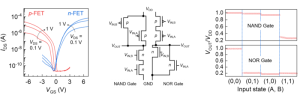
The team found it challenging to implement complementary logic circuits with conventional two-dimensional semiconductor devices because they only exhibit the characteristics of either N-type or P-type devices due to the Fermi-level pinning phenomenon.
In contrast, using the electrode material developed by the joint research team, it is possible to freely control the characteristics of the N-type and P-type devices by minimising defects with the semiconductor interface.
Improving conventional silicon semiconductors
This single device performs the functions of both N-type and P-type devices. Hence, there is no need to manufacture the N-type and P-type devices separately, such as when using a silicon-based semiconductor. By using this device, the joint research team successfully implemented a high-performance, low-power, complementary logic circuit that can perform different logic operations such as NOR and NAND.
“This development will contribute to accelerating the commercialisation of next-generation system technologies such as Artificial Intelligence systems, which have been difficult to use in practical applications due to technical limitations caused by the miniaturisation and high integration of conventional silicon semiconductor devices,” commented Dr Hwang.
“The developed two-dimensional electrode material is very thin; hence, they exhibit high light transmittance and flexibility. Therefore, they can be used for next-generation flexible and transparent semiconductor devices,” concluded Dr Hwang.