The quantum device physics laboratory leads the creation of new two-dimensional crystals inspired by graphene, targeting applications in sensing, catalysis, and nanoelectronics.
The precise control of material structure at the atomic level is at the core of modern technology. The surface of silicon carbide (SiC) provides such an opportunity: carbon atoms can be deterministically ordered, acquiring a coherent two-dimensional crystal structure over the entire SiC surface. The resulting material, so-called ‘epitaxial graphene on silicon carbide’ (epigraphene), can effectively cover entire silicon carbide wafers (6” SiC wafers are commercially available).
SiC is a wide-bandgap material; and as such it allows scalable fabrication technologies to be developed for devices without the need of transferring graphene onto another substrate. Remarkably, the technology used for epigraphene production can be tweaked to produce new two-dimensional materials beyond graphene: under certain conditions, epigraphene enables the arrangement of foreign atoms in an organised way guided by the crystalline order of graphene and the SiC surface.
We design and produce novel two-dimensional materials templated by epigraphene and study them in an integrated manner. We combine surface science studies, device microfabrication, electronic transport characterisation, and device exploration in a multidisciplinary effort that includes key researchers from Sweden at the universities in Linköping, Uppsala, Chalmers, and the MAX IV laboratory in Lund.
Epitaxial growth
Epitaxy refers to the method by which new crystals are grown on top of a crystalline substrate. In a strict sense, poly-crystalline materials (with multiple crystal domains oriented randomly) fall outside the definition of epitaxial materials. When the grown epitaxial layer consists of a different compound compared to the substrate, it is referred to as ‘heteroepitaxy’. Epitaxial growth finds commercial applications in the semiconductor industry, to produce semiconductor films on various substrates (for example silicon on sapphire, or gallium nitride on silicon carbide). Today, different epitaxial growth methods are the subject of intense research to achieve growth of two-dimensional materials over large areas.
Epitaxial graphene on SiC (Epigraphene)
Epigraphene is prepared by thermal annealing of single crystal SiC at high temperature. Today, the technology of epigraphene growth is well established at Linköping and Chalmers Universities. Growth of epigraphene proceeds via sublimation of silicon atoms from the surface of SiC; and results in an electrically semiconducting carbon buffer layer directly on top of silicon carbide, with the electrically conducting graphene layer onto the buffer.
Our team has already demonstrated a variety of applications that exploit the unique properties of epigraphene. For quantum metrology, epigraphene has become the material of choice for national metrology institutes worldwide because it simplifies and refines the electrical calibration process.1 For astronomy, we have shown a prototype epigraphene terahertz detector that could revolutionise the sensors used in next-generation space telescopes.2 For sensors, epigraphene has enabled the fabrication of Hall effect (magnetic) sensors with the lowest magnetic field detection limits suitable for operation at high temperature.3
The growth of novel two-dimensional crystals
While graphene receives a great deal of attention as a wonder-material, the carbon buffer layer is in itself a very interesting two-dimensional system. The buffer layer is also a crystalline material constituted of carbon atoms arranged in a graphene-like honeycomb structure. However, in the buffer layer, about 30% of carbon atoms are bound to the substrate, rendering the buffer a semiconducting material.
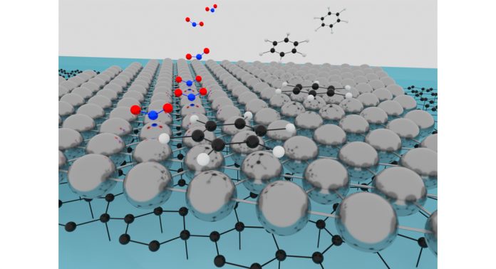
Interestingly, the carbon layers of the epigraphene system can serve as scaffolds for the (heteroepitaxial) growth of monolayer crystals of transition metal atoms. First, we have found that the buffer layer offers a unique possibility to arrange metallic atoms on its surface to form a macroscopic, electrically continuous two-dimensional layer starting from a single atom thickness. Second, it is well-established that foreign atoms can migrate underneath the surface of graphene and self-assemble at the interface between SiC and graphene. This so-called ‘intercalation process’ offers the possibility to arrange atoms in an organised way guided by the crystalline order of graphene and the SiC surface.
In our project we design, produce, and study heteroepitaxial graphene-transition metals monolayer crystals targeting strategically important directions where these novel two-dimensional materials might have substantial impact. These include:
Nanoelectronics
The interaction of graphene with heavy metal adatoms is anticipated to result in a variety of interesting physical phenomena, including topological states of matter, Moiré superlattices for twistronics, bandgap engineering in graphene, van Hove physics, etc. Producing two-dimensional graphene-metal single-layer crystal heterostructures over a large scale would allow devices to be fabricated to measure the emerging properties in quantum transport experiments.
Chemical sensors
Two-dimensional materials offer a unique platform for sensing where extremely high sensitivity is a priority, using changes in electrical conductivity used for the sensor readout. However, the sensitivity must be complemented with selectivity and, for certain applications, improved response and recovery times, as well as resilience in harsh environments. We explore two-dimensional metals to circumvent important issues with graphene-based sensors, which suffer damage during functionalisation and during operation at high temperatures or an oxidising environment. Sensors with two-dimensional metals would allow for a more robust template for functionalisation and sensor selectivity while maintaining all the advantages of high sensitivity inherent to two-dimensional systems.
Catalysis
Catalysis is employed to produce more than 90% of all chemicals used worldwide and it is critical for the development of a sustainable society. The efficiency of a catalyst, characterised by its activity, selectivity, and stability, is strongly dependent on the size and shape of the active particles and their interaction with the support material. Two-dimensional metal catalysts would allow for the detailed atomistic control over available adsorption properties, surface compositions, and chemical reaction pathways, making it possible to follow physicochemical properties of a catalyst in-situ during reaction condition. From a practical perspective, two-dimensional catalysts can lead to the ultra-efficient use of raw materials, such as scarce and expensive catalytic noble metals.
In a nutshell, our project aims at widening the family of available two-dimensional materials by integrating material design, production, and characterisation with the development of various applications. Building on a wafer-scale growth technology – epigraphene – we combine basic and applied research in two-dimensional materials to pave the road for future applications of new two-dimensional materials.
References
- Tzalenchuk, A., Lara-Avila, S., Kalaboukhov, A., Paolillo, S., Syväjärvi, M., Yakimova, R., Kazakova, O., Janssen, T. J. B. M., Fal’ko, V. & Kubatkin, S. ‘Towards a quantum resistance standard based on epitaxial graphene’. Nat. Nanotechnol. 5, 186–9 (2010)
- Lara-Avila, S., Danilov, A., Golubev, D., He, H., Kim, K. H., Yakimova, R., Lombardi, F., Bauch, T., Cherednichenko, S. & Kubatkin, S. ‘Towards quantum-limited coherent detection of terahertz waves in charge-neutral graphene’. Nat. Astron. 1–15 (2019)
- 3 He, H., Shetty, N., Bauch, T., Kubatkin, S., Kaufmann, T., Cornils, M., Yakimova, R. & Lara-Avila, S. ‘The performance limits of epigraphene Hall sensors doped across the Dirac point’. Appl. Phys. Lett. 116, 223504 (2020)
- 4 Kim, K. H., He, H., Rodner, M., Yakimova, R., Larsson, K., Piantek, M., Serrate, D., Zakharov, A., Kubatkin, S., Eriksson, J. & Lara-Avila, S. ‘Chemical sensing with atomically-thin metals templated by a two- dimensional insulator’. Adv. Mater. Interfaces 1902104, 1–7 (2020)
This project has received funding from the Swedish Foundation for Strategic Research – Stiftelsen för Strategisk Forskning (SSF).
Samuel Lara-Avila
Associate Professor
Department of Microtechnology and Nanoscience
Chalmers University of Technology
samuel.lara@chalmers.se
Tweet @chalmersuniv
www.chalmers.se/en/departments/mc2/