Deciphering the origin of the Universe through the search for ghost particles of dark matter and Majorana neutrinos requires next-generation crystal growth experiments to further reduce their background from cosmogenic induced radioisotopes.
The Big Bang Theory, which predicts matter-antimatter symmetry in the infant Universe, is widely accepted to explain the origin and early evolution of the Universe. However, observational evidence indicates the structure of the Universe today is matter dominant. Consequently, the matter-antimatter symmetry was broken through an unknown physics process. This is a compelling mystery. Furthermore, experimental evidence suggests 80% of matter is dark matter, which does not shine or reflect light. Despite great efforts made so far, dark matter continues to have a ghostly nature. Germanium (Ge)-based experiments have the lowest detection energy threshold in the search for dark matter amongst large-scale experiments.
Majorana neutrinos (neutrino and antineutrino are the same particle) may shed light on the physics process that broke the matter-antimatter symmetry, if they are proven to exist. The only practical way to prove neutrinos are Majorana particles is to detect neutrinoless double-beta decay. This is a non-standard form of nuclear decay and only a handful of nuclei can undergo this decay process. 76Ge-based detectors possess the best energy resolution to discover this rare decay process. Therefore, Ge-based experiments are vital in searching for ghost particles of dark matter and Majorana neutrinos. However, cosmogenically produced long-lived radioisotopes can undermine the detection goal and hinder the discovery sensitivity.
Underground crystal growth and detector development can largely reduce cosmogenic processes and hence maximise the discovery potential in detecting dark matter and proving the existence of Majorana neutrinos. This means Ge purification, Ge crystal growth, and Ge detector fabrication should be implemented in an underground environment where the experiments will be built.
Ge material
Ge is a rare element in the Earth’s crust. The abundancy of Ge is estimated to be in the level of ~7 ppm. The production of Ge is mainly from zinc ore processing and coal fly-ash extraction. Natural Ge consists of five isotopes: 70Ge (20.52%), 72Ge (27.45%), 73Ge (7.76%), 74Ge (36.52%), and 76Ge (7.75%). Ge is a semiconductor material, which has a variety of applications in industry including electronics, fibreoptic systems, infrared optics, polymerisation catalysts, and solar applications. Commercially available Ge ingots have impurity levels ranging from 99.99% to 99.999%. Even the highest level of impurity commercially available is unacceptable to grow Ge crystals aimed to make Ge detectors. Therefore, commercial ingots must be purified to a level of 99.999,999,999,9% to grow a Ge crystal, of which a portion has a chance to reach the impurity level necessary to produce a detector-grade crystal with an impurity level of 99.999,999,999,99%.
Ge purification
Ge is purified using a process called zone refining, which creates a melting zone to move from one end of the Ge ingot to the other. This process was first developed in Bell Labs in 1954. During the process of zone refining, the impurities are segregated at the boundary between the liquid and the solid of the melting zone. Impurities stay in the melt and move to the end. After many passes, impurities are concentrated in the end of the Ge ingot. Once the end portion is cut off, a large portion of the Ge ingot has its purity increased. Depending on the quality control (the optimisation of the multiple influential parameters) and the number of passes, zone refining can purify Ge ingots from 99.999% to 99.999,999,999,9% – a reduction of seven orders of magnitude. The purified Ge ingots can then be used for Ge crystal growth. After 12 years of research and development (R&D) on the surface lab, the University of South Dakota (USD) has established a standard procedure that ensures high yield (~80%) of the purified Ge ingots meet the requirements (a seven orders of magnitude reduction of impurity) of crystal growth.

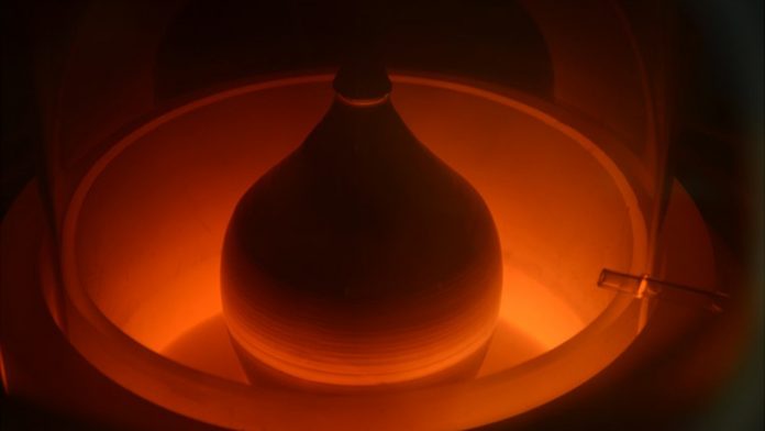
Ge crystal growth
Large-size Ge crystals are grown with the Czochralski technique, which was developed in the 1930s. Crystal growth is an art. The crystal growth involves heat, momentum, and mass transport phenomena, chemical reactions (e.g., crystal and melt contamination) and electro-magnetic processes (e.g., induction and resistance heating, magnetic stirring, magnetic breaks, etc.). Consequently, the dynamic crystal growth process involves phase transformation from liquid to solid. The interface control between liquid and solid is on the scale of nanometres and the growth system is on the order of ~meter size. This requires numerous parameters (ten or more) to be optimised with many constraints. Therefore, the dynamic character of the crystal growth process is very difficult to control. The growth rate and quality of high-purity Ge crystals largely depend on the control of the thermal field (heat transfer and temperature profile). However, these control parameters can only be regulated externally. More specifically, they can only be regulated through growth system geometry, gas flow rate and pressure, pulling rate, frequency, and the power of the RF heater. Measurements inside the growth chamber (temperature over 1000oC), and a quantitative determination of the control parameters are technically challenging. With 12 years of R&D on the surface lab, USD has invented a growth method that has facilitated detector-grade crystal (99.999,999,999,99%) production on a regular basis. This paves the way for growing Ge crystals underground.
Crystal characterisation
Characterising grown crystals provides feedback for the growth process and helps determine whether crystals are of sufficient quality to be used in the fabrication of detectors. With 12 years R&D experience, USD has created a rich characterisation programme to determine which crystals meet the qualifications for detector fabrication. The quality of a single-crystalline Ge crystal is determined through X-ray diffraction and dislocation density measurements using an optical microscope. The impurity level is determined by Hall Effect measurements; purity of the grown crystal is confirmed by identifying shallow impurities using Photothermal Ionization Spectroscopy (PTIS) and natural impurities with Inductively Coupled Plasma Mass Spectrometry (ICP-MS). Additional knowledge and techniques for characterising grown crystals can be obtained by using diverse, established characterisation techniques.
An advanced van der Pauw Hall Effect measurement system, capable of testing samples with variable temperature from 77K up to 300K, can be carried out. We can also employ a deep level transit spectroscopy system that will enable identification of deep level impurities in grown crystals. This set of the characterisation tools allows us to have a comprehensive understanding of the grown crystals for developing novel detectors, whose performance strongly depends on crystal properties including shallow/deep level impurities, dislocation density, and defects.
Detector fabrication
Utilising the grown crystals, USD and its collaborators can fabricate Ge detectors in different geometries including planar detectors, point contact detectors, and ring-contact detectors with different contact technologies. Commercially available Ge detectors are made with lithium diffusion as n+ contact and boron implementation as p+ contact. The basic principle is to create charge barrier height through a traditional p-n junction technology.

More recently, the scientists at Lawrence Berkeley National Laboratory have invented bi-polar blocking technology using amorphous Ge and amorphous Si as detector contacts. This technology creates thin contacts (~600 nm) on Ge in comparing to Li-diffused thick contact (~1 mm). One of the advantages for thin contacts is to make segmented Ge detectors. USD has the capacity to make thin-contact detectors using sputtering technology. After five years R&D, USD has established detector fabrication capacity and demonstrated thin-contact technology with the USD-grown crystals.
The USD surface laboratories
The in-house Ge detector production chain from Ge zone refining, crystal growth, crystal characterisation, and detector fabrication has been established at USD since 2010. A grant from the state of South Dakota created Governor’s Research Center for ultra-low background experiments in the Dakotas (CUBED). Using these funds, USD was able to start the exploration of Ge crystal growth in the surface labs. Soon after, a grant from the Department of Energy’s Established Program to Stimulate Competitive Research (EPSCoR) funded the crystal growth and detector development programme in South Dakota through its implementation award. This grant allowed USD to quickly move forward for a full capacity of R&D to build up the production chain of Ge detectors.
The South Dakota Board of Regents and USD invested significant funds to renovate a lab space of ~6600 square feet and facilitated the required power, water, and gas pipes to grow Ge crystals and develop Ge detectors. More recently, the National Science Foundation funded an international team led by USD through Partnerships for International Research and Education (PIRE) to continue Ge crystal growth and detector development. All of the above contributed to making the USD surface labs available to transfer technology to underground for Ge purification, crystal growth, crystal characterisation, and detector development.
Please note, this article will also appear in the twelfth edition of our quarterly publication.