Dr Eva Vilella-Figueras, UKRI Future Leaders Fellow at the University of Liverpool, speaks to The Innovation Platform about the revolutionary HV-CMOS silicon sensors her team are developing for fundamental physics experiments.
Dr Eva Vilella-Figueras, who since 2017 has led the CMOS working group within RD50 – the CERN collaboration dedicated to the development of extreme radiation-tolerant sensors for future high luminosity colliders – is aiming to obtain enhancements in the performance of HV-CMOS sensors in commercially available processes. She spoke to The Innovation Platform about how these sensors, which are currently undergoing further testing to achieve their optimum efficiency, potentially have an extensive plethora of applications for physics experiments, including HL-LHC upgrades, FCC, pEDM, Mu3e, and g-2, in addition to other fields such as healthcare.
H2 What are HV-CMOS sensors?
CMOS (Complementary Metal-Oxide-Semiconductor) is one of the most popular commercial process technologies available to fabricate integrated circuits such as microprocessors, memory devices, and image sensors used in mobile phones and digital cameras. HV-CMOS (High Voltage-CMOS) is a variant of standard CMOS process technologies, which allows a large voltage (for example, 100 V) on the device. HV-CMOS is widely used to manufacture power management devices, such as controllers for electric motors and displays. HV-CMOS is also an extremely attractive option for producing silicon sensors to measure charged particles in physics experiments.
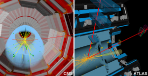
In large particle physics experiments, such as those at the Large Hadron Collider (LHC) at CERN, billions of collisions per second produce thousands of billions of particles. These particles pass through several layers of silicon detectors that surround the collision point. If a particle carries an electric charge, it will leave a trace in each layer of silicon. Similar to how conservationists use footprints on snowy paths to track and identify animals, physicists use traces in silicon detectors, like HV-CMOS, to reconstruct particle trajectories (known as particle tracking) and identify them. However, particle tracking is technologically very challenging. To simplify this problem, physicists need extremely fast and thin sensors with tiny sensing cells that measure accurate tracepoints while dissipating little power. Radiation tolerance and cost are also critical, as sensors have to survive many years of operation and typically cover several square meters.
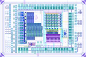
HV-CMOS is the only sensor technology to date that shows great potential in fulfilling all the requirements outlined above. There is no other sensor technology that currently has the same promise. Silicon sensors require a sensing cell, which generates a small electric signal when a charged particle traverses it, and readout electronics to amplify and record this electric signal. HV-CMOS sensors integrate the sensing cell (pixel) and advanced readout electronics in a single layer of silicon that is as thin as a human hair. At the same time, HV-CMOS sensors also provide good tracepoint resolution (a 2cm x 2cm sensor chip contains about 50,000 pixels), fast-timing capability, excellent radiation tolerance, and affordable cost per area. HV-CMOS sensors are emerging as a prime candidate to measure charged particles in many future physics experiments due to all these significant advantages.
What are their applications?
HV-CMOS sensors are being developed mostly to measure charged particles in next-generation physics experiments that will create extremely challenging environments and require high-performance silicon tracking detectors. HV-CMOS sensors have found applications in other fields as well, such as medicine, astrophysics, and microscopy.
The Mu3e experiment at the Paul Scherrer Institute (PSI) in Switzerland is searching for direct evidence of completely new physics beyond the Standard Model and is currently in its construction phase. It will be the first application of HV-CMOS sensors. For the Mu3e experiment to succeed, the silicon tracking detector has to meet extreme requirements, especially in terms of thickness (50 µm), pixel size (80 µm x 80 µm) and timing capability (better than 20 nanoseconds). HV-CMOS are the only silicon sensors that presently meet all these requirements.
HV-CMOS sensors are also being considered for several other physics experiments, such as the LHC beauty (LHCb) experiment at CERN and Electric Dipole Moment (EDM) searches at the Cooler Synchrotron (COSY) in Germany. The LHCb experiment, which specialises in investigating the matter-antimatter asymmetry of the Universe, will undergo a series of planned detector upgrades in the coming years to intensify its potential for new discoveries in the so-called HL-LHC (High Luminosity-LHC). A new detector, called ‘Mighty Tracker’, is proposed to be installed in LHCb as part of these upgrades.
The Mighty Tracker would use HV-CMOS sensors to meet the anticipated requirements on point resolution, radiation tolerance, and cost. The ability to have a relatively high point resolution has been found to provide significant advantages for the track reconstruction. EDM is a measure of the separation of positive and negative charge distributions within a particle. Its value is essentially zero according to the Standard Model; however, new theories predict the existence of a permanent non-zero EDM which would be a univocal sign of new physics. To probe into that, HV-CMOS sensors are proposed to achieve unprecedented accuracy and minimal material thickness that this experiment requires.
Another application of HV-CMOS sensors is in proton beam therapy, a radiotherapy modality that uses protons to treat certain types of cancer. Proton beam therapy has considerable advantages over conventional radiotherapy, which uses photons to accurately target tumours inside the body without damaging a patient’s healthy tissues. As a result, many new centres offering this treatment are currently being built around the world. Proton beam monitor technology is essential to verify the compliance between the prescribed and delivered treatment. Following extensive research carried out for physics experiments, HV-CMOS sensors are being developed to measure the energy loss of protons after they pass through the patient, which will result in better outcomes for patients.
How can HV-CMOS sensors improve the instrumentation at CERN?
The most common tracking sensor technology used today in physics experiments with high particle rates is based on a hybrid model. Hybrid detectors are named to reflect their composite nature; the sensing cell or pixel and the readout electronics are two separate entities (in two separate layers of silicon) and connected via tiny conductive bumps using flip-chip bump-bonding techniques.
Hybrid detectors offer the advantage of tailoring the design of the sensing device to tolerate very high integrated particle fluence. However, due to their multi-layer nature, hybrid detectors require substantial material thickness, limiting the accuracy with which particle trajectories can be measured. The bump-bonding process to connect the pixels to the readout electronics also imposes a minimum pixel size, making it impossible for these detectors to achieve the very fine point resolution necessary to resolve the many millions of particle trajectories expected at the highest rate future experiments. Moreover, bump-bonding is complex and comes with prohibitive costs. The approximate cost of instrumenting 1m2 with hybrid detectors costs £1M, and tracker detectors in future experiments will require many square meters.
CMOS process technologies can also be used to produce silicon sensors for physics experiments. CMOS sensors integrate the sensing element and readout electronics in a single layer of thin silicon, which removes the need for interconnection with solder bump technology. CMOS sensors, however, cannot achieve sufficient readout speed and radiation tolerance to be a viable option for the high rate particle tracking required in most state-of-the-art experiments. Nonetheless, these detectors have been successfully employed in a subset of experiments, like the upgrade of the ALICE experiment at the LHC, where lower readout speeds and moderate radiation tolerance are acceptable.
HV-CMOS sensors integrate the best of hybrid and CMOS sensors. They provide fast-timing capability and excellent radiation tolerance like hybrids; they are also thin, with very small sensing cells for good tracepoint resolution, and are more affordable like CMOS sensors. HV-CMOS sensors are the strongest candidate technology to meet all the performance requirements for future experiments. There is now a wide consensus within the community that HV-CMOS sensors will replace hybrid sensor technologies in next-generation physics experiments.
What are the goals of the HV-CMOS research and development programme?
Despite the major improvements already demonstrated by HV-CMOS sensors, the enormous challenges set by future physics experiments demand substantial further research to achieve further enhancements. The main goal of our research and development programme is to push the boundaries of HV-CMOS sensors to achieve a step-change improvement in their performance, especially in terms of single tracepoint resolution (micron-scale), fast-timing capability (one nanosecond), and radiation tolerance (extreme levels).
We also pursue the deployment of HV-CMOS sensors in the most ground-breaking future physics experiments (for example, HL-LHC upgrades, Mu3e upgrade, EDM, and g-2, among others) to enable exciting discoveries (for example, finer studies of the Higgs boson and new studies of lepton flavour violations, dark matter, and dark energy), and also in other areas where these sensors can make a significant impact like proton beam therapy for cancer treatment.
How close are you to achieving these goals?
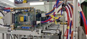
To accomplish the HV-CMOS research and development programme, my group at the University of Liverpool and I design HV-CMOS sensor prototypes, submit them for fabrication to commercial vendors, and evaluate their performance. The design phase includes performing device simulations to anticipate the behaviour of the sensor and complex readout electronics prior to their fabrication, laying out their physical implementation, and running extensive verifications to prevent potential mistakes, all using advanced design tools.
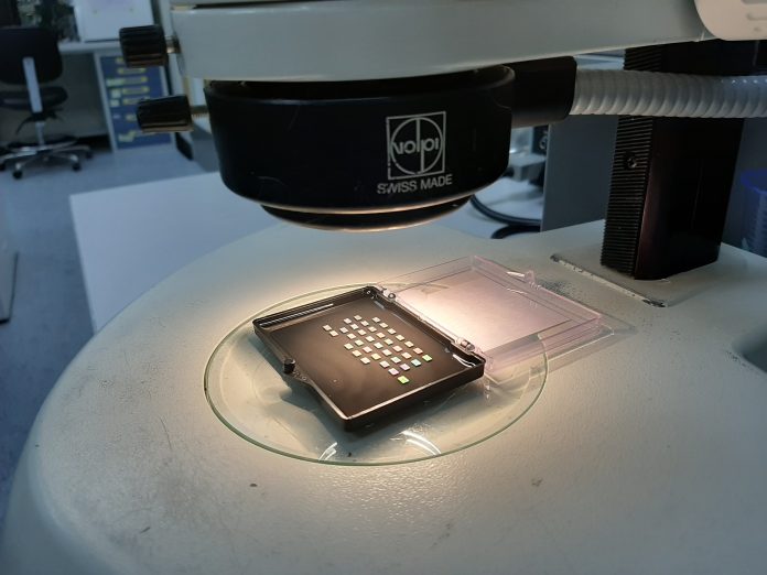
We run physical simulations of HV-CMOS sensors in physics experiment environments to understand how the devices will behave in their final application and guide their design. After the delivery of the fabricated samples, we perform a wide range of measurements (for example, electrical tests to measure the speed and power consumption) both in the clean rooms at Liverpool and in international facilities, such as CERN, where we have access to beams of high energy particles. We measure the samples before and after irradiation with protons and neutrons.
We will soon receive a new sensor prototype, called ‘UKRI-MPW0’, which my research group fully developed at Liverpool and which incorporates a new sensor implementation with methods aiming to boost the radiation tolerance. The new sensor implementation has the potential to hit all three targets of the HV-CMOS research and development programme at once (good tracepoint resolution, fast-timing capability, and high radiation tolerance), but this will have to be verified and confirmed through extensive performance evaluation measurements. If this prototype performs according to our expectations – which we fully tested through simulations before submitting the design for fabrication – then our next step will be to design a new prototype that will incorporate all the lessons learnt with UKRI-MPW0 plus sophisticated interface readout electronics to optimise the transmission of the data generated by the sensor.
The HV-CMOS research and development programme is funded through a Future Leaders Fellowship from UKRI (UK Research and Innovation). It is a prestigious and exciting new scheme that aims to develop, retain, attract, and sustain research and innovation talent in the UK. The long-term, flexible funding this scheme provides has allowed me to form and develop a leading research group and given me access to the necessary resources to tackle the difficult challenge of achieving a step-change improvement of HV-CMOS sensors.
Please note, this article will also appear in the sixth edition of our quarterly publication.