An interface-templated method has the potential to enhance the crystallinity of large single-layer graphene sheets on insulating supports.
A novel method can improve the crystallinity of large single-layer graphene, by electrically insulating its supports. This potentially could help with the development of next-generation nanomaterial-based devices, such as very light and thin touchscreens, wearable electronics and solar cells.
The majority of graphene-based electronic devices require insulating supports. However, high-quality graphene films designed for industrial use are typically grown on a metal substrate, such as copper foil, before being transferred to insulating support for device fabrication. This transfer phase can introduce impurities that affect how well the device performs. Previous endeavours to grow graphene on insulating supports have not been able to produce the required high-quality single crystals.
“If graphene can be grown on an insulating substrate with a clean interface, certain devices might function better,” explained PhD student Bo Tian, who co-led the study under Xixiang Zhang’s supervision. “This also opens the door to new types of graphene-based nanodevices.”
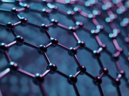
Enhancing the crystallinity of large single-layer graphene
Zhang, Tian and co-workers from Asia and Europe tweaked the chemical vapour deposition method, which relies on the copper-catalysed decomposition of methane into carbon precursors, to generate smooth single-crystal graphene monolayers on wafer-scale single-crystal substrates called c-plane sapphire.
The researchers converted polycrystalline copper foil into its single-crystal counterpart Cu (111) on the sapphire surface and introduced active carbon atoms from the metal substrate-catalysed decomposition of methane on the resulting film. The carbon atoms diffused through the metallic film toward the copper–sapphire interface, which acted as a template, and formed well-oriented graphene islands that, after several growth cycles, merged to yield a sheet.
In addition to weak surface interactions, the copper film and sapphire displayed similar crystal lattice symmetry to that of graphene, which explains the high crystallinity of the graphene monolayer.
Carbon diffusion
The researchers etched away any graphene that had accumulated on top of the copper film using a hydrogen–argon plasma to facilitate carbon diffusion. They immersed the samples in liquid nitrogen before heating them rapidly to 500 oC, making the copper film easy to peel off while keeping the graphene monolayer intact.
Field-effect transistors manufactured on the sapphire-grown single-crystal graphene monolayer exhibited excellent performance with higher carrier mobilities. The superior electronic performance of the graphene that is grown on sapphire, results from its higher crystallinity and fewer folds on the surface.
“Our team is now trying to grow other two-dimensional materials on the insulator-supported graphene to build functionalised large-scale heterostructures,” explained Tian. These heterostructures held together by van der Waals interactions are expected to be useful in future nanodevices.