Masahiro Goshima, from the National Institute of Informatics, speaks to The Innovation Platform about the unique characteristics of their clocking scheme for semiconductor circuits.
As cars are made mainly of iron, computers are made mainly of semiconductors. Unlike other materials such as iron, semiconductors have shown an exponential improvement, known as Moore’s Law. Circuit and architecture technologies have played a role in leading the exponential improvement of semiconductors into an exponential improvement of computers.
Because the improvement of semiconductors has been so impressive, even professional computer scientists can make the mistake of thinking that this is the main cause of the similar improvement of computers. However, that is incorrect. In the 1990s, processors were developed which were ten times faster than their predecessors, with the same speed improvement seen in their clock speeds. However, while their clock speeds have remained almost the same (about 4GHz) since that time processors, on the other hand, have once again improved by a factor of ten once more. This means that the state-of-the-art processors can now execute ten times more instructions in a clock cycle than those from 16 years ago.
Computer architects have funnelled the exponential improvement seen in semiconductors to the clock speed of the 1990s, and thus to the efficiency in this century. Although the source of the exponential improvement of computers is the exponential improvement of semiconductors, this cannot be realised without circuit and architecture technologies. Indeed, even after the end of Moore’s Law, computers will continue to improve with circuit and architecture technologies.
Random variation
Although it is generally considered that Moore’s Law is coming to an end, its scientific basis, ‘Dennard scaling’, actually ended at the beginning of this century. While Moore’s Law focuses on the feature sizes of the transistors in semiconductor chips, Dennard scaling also takes into consideration the power supply voltage of them. Dennard scaling roughly states that the supply voltage should be scaled down in proportion to the feature sizes. However, it has not been possible to scale the power supply voltage from 1V or lower, and the power consumption and the resultant heat have been the main factors limiting semiconductor performance.
One of the main reasons is random variation in semiconductor manufacturing. Variation in semiconductor manufacturing can be categorised into systematic and random variations. Among them, random variation is becoming dominant because the feature sizes of transistors in semiconductor chips has become closer to the sizes of the atoms. As a result, random variation as small as one atom has non-negligible effect on the performance of a circuit element, such as wires and transistors.
Therefore, it is essentially difficult to solve this problem by semiconductor manufacturing technology, and circuit and architecture technologies are needed to mitigate the problem. Our clocking scheme is one of such technologies to tackle this problem.
Random variation and worst-case design
Increase of random variation affects the performance of semiconductor circuits through worst-case design. To date, worst-case design has been widely accepted. Here, semiconductor circuits are designed so that they work even if all the circuit elements had worst-case delays. However, this estimation is extremely pessimistic, because the probability that all the circuit elements in a circuit path have the worst-case delays is extremely low. The worst-case design has worked only because the worst-case delays were not so far from the typical-case delays. We cannot expect the same performance improvements as seen in the past with the worst-case design.
To deal with this problem, a wide variety of methods have been considered. For example, statistical static timing analysis is introduced to relax the extremely pessimistic estimation.
Timing fault detection
A timing fault is a transient fault caused by dynamic variation in the circuit delay. In the worst-case design, large scale integrations (LSIs) are designed so that a timing fault does not occur even in the worst cases. Therefore, timing faults can only occur in unexpected situations such as thermal runaway caused by a failure of the thermal sensor.
The timing fault detection techniques with dynamic voltage and frequency scaling (DVFS) gives us a hint as to how we can transcend the problem of worst-case design. That is, a device operates with a lower voltage and/or a higher frequency than given by the worst-case design. As a matter of course, a timing fault occurs, which goes on to be detected by a detection circuit. Then, the device is recovered to a fault-free state. The voltage and frequency will be configured so that the fault rate becomes sufficiently low.
In this way, the device operates with the actual delay according not to the worst case but to the actual operating environment of the individual device, and thus to the actual performance of the individual device. However, the ability of this simple timing fault detection to random variation is quite limited.
Our clocking scheme
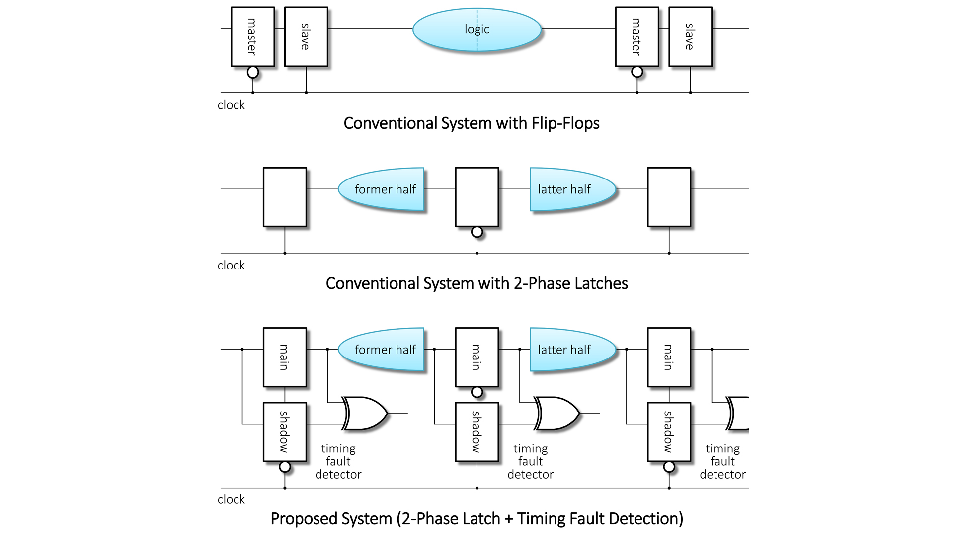
The clocking scheme that we have developed is a way to make the digital signals proceed one stage of a circuit in a cycle of the clock signal. There are two major clocking schemes: Flip-Flop (FF) with single-phase clock, and latch with two-phase clock. Though their performances are not very different for usual use, the FF scheme is more design friendly. Thus, almost all the digital circuits in the real world adopt the FF scheme, and the latch scheme has almost disappeared.
However, we use the latch scheme as the basis of our clocking scheme. As shown in the circuit diagrams, a conventional circuit for FFs is converted into a circuit for latches with timing fault detectors. This combination of the latch scheme and timing fault detection realises behaviour based not on the worst but on the typical case.
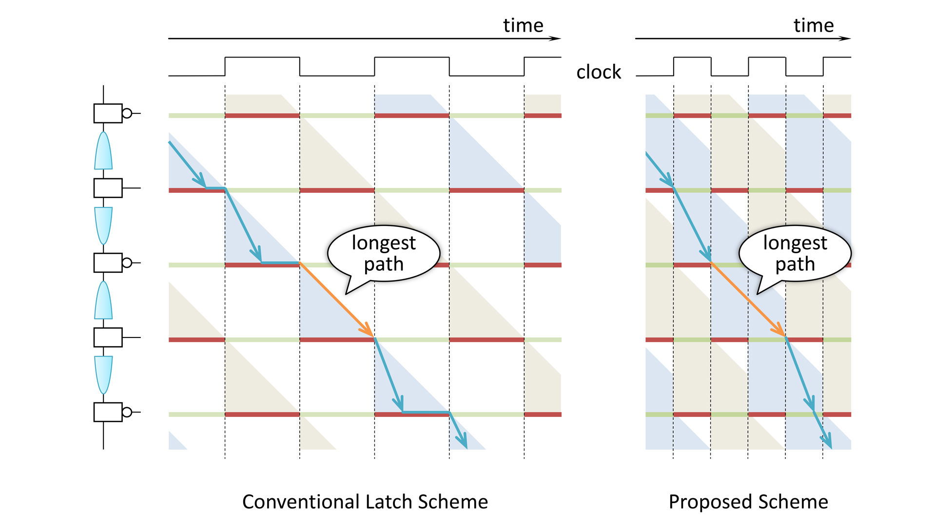
If digital signals flowing in a circuit were compared to cars running on roads, the open/closed latches could be compared to green/red traffic lights, which are represented by the green/red horizontal bars in the timing diagram. The traffic lights are controlled by the clock signal. A single clock signal is provided for the lights, and it should be controlled so that every car proceeds one section in a cycle time of the clock signal. As shown in the diagram, when a light turns green, the next light turns red at the same moment.
In each section between two successive lights, there are many short paths and a few long paths. The possibility of the worst case, i.e., the possibility to take the longest path is as small as 1%. In addition, the lengths of the paths randomly vary because of the random variation.
As stated above, when a light turns green, the next light simultaneously turns red. Thus, even if a car takes a short path and arrives at the next light earlier, it must necessarily wait there. The light must turn green after the last possible car that takes the longest path arrives there.
Thus, the cycle time of the clock for the lights is given by the longest path length in all sections, i.e., the worst case concerning the path selection. In addition, because this longest path length varies due to the random variation, the cycle time is also given by the estimated worst case concerning the random variation. In other words, the cycle time of the clock is given by this worst-of-the-worst-case value. The waiting time of the car that arrived earlier cannot be utilised.
Timing fault detection can shorten this cycle time to better than the worst-of-the-worst-case value because it safely manages the case for when a car cannot arrive in time. However, as stated before, the ability of timing fault detection with FFs to random variation is quite limited. In this case, timing faults occur too frequently and the penalty for recovery can nullify the gain.
Dynamic time borrowing
Our scheme overcomes this problem. We found the following phenomenon when timing fault detection is applied to the latch scheme, which we name ‘dynamic time borrowing’. In our scheme, as the cycle time is shortened, the lights turn green earlier. Then, a car that takes a short path arrives at a green light earlier and can proceed to the next section without waiting. Then, even if the car takes a long path in the next section, it will be able to arrive at the next light in time, i.e., without timing fault. The variation concerning the path selection is accommodated among sections. In this fashion, the cycle time of the clock for the lights is decided not by the longest path lengths but by the average path length, which is much shorter than the longest paths.
In addition, this phenomenon has an effect to mitigate random variation. When a car passes n paths of n sections without waiting on lights, it is equivalent to that the car passes a single longer path composed of the n paths of the n sections in n cycles. As n increases, the random variation of the single longer paths approaches zero by the Law of Large Numbers.
In our scheme, the lower limit of the clock cycle is given by the limit to correctly detect timing faults and decreased by the half from the conventional FF scheme. This timing budget can also be used to lower the supply voltage.
Conversion algorithm
As stated above, almost all of the circuit is designed for FF. It is therefore desirable to automatically convert circuits for FFs into equivalent circuits for latches. As shown in the circuit diagrams, this can essentially be performed by cutting them into the former and the latter halves.
The circuits should be cut down the middle. This problem looks like but is not the so-called ‘minimum cut problem’. We found that the solution of conventional minimum cut algorithms is not applicable for digital circuits
For a number of years, we unsuccessfully employed a heuristic search before finally developing an algorithm to apply conventional algorithms for the minimum cut problem to our own problem. We went on to develop a circuit conversion program with this algorithm and applied it to a processor (described below).
Application to Rocket processor
We are evaluating our scheme with an FPGA. An FPGA (Field-Programmable Gate Array) is a semiconductor device that can be programmed for different implementation after fabrication.
We are applying our clocking scheme to the Rocket processor implemented in the FPGA. The Rocket processor is a RISC-V scalar processor originally developed at UC Berkeley.
Basically, recovery from a timing fault is realised on the basis of the processor context, which is generally used for the context switch in usual multi-process operating systems such as Windows or Linux. A timing-fault-tolerant processor protects its context from faulty updates possibly affected by timing faults. On a timing fault, it can restart from that non-faulty context after re-initialising the other parts than to save the context.
We modified the Rocket processor so that it can recover from a timing fault. Because the Rocket processor has a gimmick in updating the processor context for more performance, we had to disable it. The modified Rocket processor in the FPGA can boot Linux and recover form timing faults injected from a toggle switch on the FPGA board.
We have a plan to make a silicon prototype device of a processor using a shuttle service in order to evaluate our scheme with real devices. One of these processors will be a RISC-V compliant superscalar processor we designed.
Conclusion
This article describes our clocking scheme that can mitigate the random variation problem which semiconductor manufacturing faces.
This scheme can decrease the cycle time by the half from the conventional clocking scheme. The method is applicable for almost all digital circuits including processors. If our method is applied to Intel or AMD x86 processors, they can achieve 10GHz clock speed in boost mode. This timing budget can also be used to lower the supply voltage.
Masahiro Goshima
Professor
National Institute of Informatics
+81 3 4212 2545
goshima@nii.ac.jp
Tweet @jouhouken
https://www.nii.ac.jp/en/faculty/architecture/goshima_masahiro
Please note, this article will also appear in the second edition of our new quarterly publication.