Researchers have developed a new technique for alleviating electromigration in nanoscale electronic interconnects, enhancing the durability of future integrated circuits.
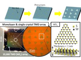
The discovery, made by scientists from the University of South Florida, entails encasing copper metal interconnects with hexagonal boron nitride (hBN), a material similar to graphene that is automatically thin, insulating, and two-dimensional, which successfully mitigates electromigration.
Their research is published in the journal Advanced Electronic Materials.
Electromigration is a process that instigates device failure, occurring when an electrical current permeating through a conductor causes the atomic-scale erosion of the material; although modern semiconductor technology utilises a barrier or liner material to solve this problem, crucial space is wasted in the technology by doing so that could be better used for additional transistors.
This novel approach achieves this feat by employing the worlds thinnest materials – a nanometre is 1/60,000 the thickness of a human hair, with an ångström being one-tenth of a nanometre saving vital space within the technology.
Professor Michael Cai Wang, the leader of the research from the University of South Florida, said: “This work introduces new opportunities for research into the interfacial interactions between metals and ångström-scale 2D materials. Improving electronic and semiconductor device performance is just one result of this research.
“The findings from this study opens up new possibilities that can help advance future manufacturing of semiconductors and integrated circuits. Our novel encapsulation strategy using single-layer hBN as the barrier material enables further scaling of device density and the progression of Moore’s Law.”
Their analysis demonstrated that the neoteric method achieved more than 2500% longer device lifetime, far exceeding the current density of comparable control devices by 20%, with further potential for additional densification of the integrated circuits, boosting device efficiency and reducing energy consumption.
Yunjo Jeong, the first author of the study, explained: “With the growing demand for electric vehicles and autonomous driving, the demand for more efficient computing has grown exponentially. The promise of higher integrated circuits density and efficiency will enable the development of better ASICs (application-specific integrated circuits) tailored to these emerging clean energy needs.”
This groundbreaking innovation could have a wide range of applications, with modern cars requiring hundreds of microelectronic components, meaning that minimising the electromigration of these integrated circuits will further boost their efficiency.
“Our findings are not limited only to electrical interconnects in semiconductor research. The fact that we were able to achieve such a drastic interconnect device improvement implies that 2D materials can also be applied to a variety of other scenarios.” Wang commented.