
Ultrathin layers and ordered nanocylinder arrays in solar cells made from alternative materials.
With his ERC Grant ‘Solacylin’, Professor Julien Bachmann and his team at the University of Erlangen control interfaces in photovoltaic devices for optimised performance on the basis of simple materials and simple processing methods.
The vast majority of solar cells available commercially nowadays features strictly planar interfaces between layers of highly pure semiconductors such as 99.9999% silicon or ‘CIGS’ (a copper indium gallium sulfide/selenide) and cadmium sulfide. These materials are generated as bulk crystals or as rather thick (>100 nm) films by expensive and energy-intensive cleanroom or ultrahigh vacuum processing. In his Consolidator Grant project ‘Solacylin’ funded by the European Research Council (grant agreement 647281), Professor Julien Bachmann, chair for ‘Chemistry of Thin Film Materials’ (CTFM) at the Friedrich-Alexander University of Erlangen-Nürnberg in Germany, explores creative ways to circumvent the need for such expensive materials and methods.
The long-term vision is that a smart engineering of the interface between two adjacent semiconductors might enable one to exploit materials of inherently lesser quality to devise photovoltaic devices featuring a reasonable performance nevertheless. This interface engineering can take two distinct forms, which can be combined:
1) fine-tuning the chemical identity and physical properties of the interface with ultrathin layers of near-atomic thickness
2) adjusting the geometric area of the interface and the transport paths of charge carriers in its vicinity with ordered arrays of coaxial, nanocylindrical junctions.
Preparative methods
The method of choice in the CTFM lab for generating both ultrathin (≤2 nm) and somewhat thicker (2-80 nm) layers, including coatings of non-planar substrates, is atomic layer deposition (ALD). ALD is a coating technique based on the exploitation of two (or more) complementary surface reactions performed sequentially and occurring in a self-limiting manner. Each such reaction step results in depositing a well-defined amount of solid (corresponding to an atomic monolayer or less) and terminates the surface with a distinct type of reactive groups. After the original chemical identity of the surface has been regenerated upon completion of the two (or more) steps, these steps are repeated in a cyclic manner until a desired thickness is reached. Moreover, because the amount of material deposited at each cycle is controlled by the surface chemistry and not by mass transport of precursors from the fluid phase, coatings or pores feature a constant thickness along the whole pore length.
A significant development of ALD achieved in the framework of ‘Solacylin’ is its generalisation from gaseous precursors (which were the norm since the method was invented four decades ago) to dissolved ones. The exploitation of the liquid phase allows one to increase the range of precursors applicable to ALD coatings significantly in ‘solution ALD’ (sALD). For example, ionic compounds may be used as precursors from the solution phase, while they do not provide the vapor pressure required for regular gas ALD. In particular, scientists in the CTFM laboratory are currently exploring sALD as a method for the deposition of ionic semiconductors such as the hybrid perovskites which have proven particularly exciting in the photovoltaic community recently.
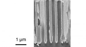
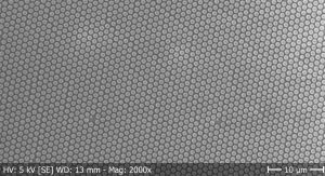
ALD can then be combined with a variety of nanostructured templates in order to generate corresponding interfaces (Fig. 1). The Solacylin project relies on ‘anodization’, the electrochemical oxidation of electropositive metals, to generate cyclindrical pores of controlled geometry in self-ordered arrays. Method development has been necessary in order to transfer the well-established methods, which start from bulk pieces of metal, to films deposited on the transparent electrodes needed to build solar cells. For example, the self-assembly of nanosphere monolayers is exploited to control the order in such thin anodic layers (Fig. 2).
Ultrathin interfacial layers in antimony sulfide cells
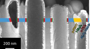
One material system investigated in the Solacylin project bases on titania (TiO2) as the electron transport material, antimony sulfide (Sb2S3) as the undoped light absorber, and polythiophenes such as P3HT (poly-3-hexylthiophene) as the hole transporters. The high purity of ALD-deposited Sb2S3 has uncovered an inherently poor adhesion between TiO2 and Sb2S3, presumably related to the moderate affinity of antimony (III) for the oxide ion, and conversely of titanium(IV) for sulfide.
This chemical incompatibility has been circumvented by the introduction of an ultrathin ZnS interfacial layer. Its presence, even in a thickness as low as one single nanometer or less (a few atoms thick) suffices to generate sufficient adhesion and enable the formation of continuous, thin Sb2S3 coatings on titania, both in planar geometry and inside the straight ‘anodic’ alumina pores (Fig. 3). In physical terms, this layer behaves as a tunnel barrier.
Nanostructured interfaces in perovskite cells
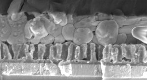
The CTFM team members have also managed to transfer their coating and infiltration methods to hybrid perovskite materials of the haloplumbate family, with methylammonium iodoplumbate (‘MAPI’) as the most prominent example. Fig. 4 displays such a cell in which an array of titania nanotubes has been defined directly on a transparent electrode and complemented with MAPI and an organic hole transporter (whereas gold has been placed as the second electrode). The performance of these devices depends on the geometry of the tubes in a systematic manner, which reveals how their overall solar energy conversion efficiency can be improved in the future. Further recent efforts in the Solacylin project have been dedicated to the replacement of lead-based materials by alternatives, in particular based on sALD. In the near future, the Solacylin team members hope to deliver stable solar cells based on abundant elements in non-toxic semiconductors, deposited with atomic precision by solution processing.
Professor Julien Bachmann PhD
Chair
Chemistry of Thin Film Materials
Department of Chemistry
and Pharmacy
Friedrich-Alexander University of Erlangen-Nürnberg
+49 9131 85 70551
julien.bachmann@fau.de


