Researchers from the Universität Bochum (RUB) and the Technical University of Munich (TUM) have developed a technique to improve the manufacturing process of producing quantum dots.
Quantum dots are semiconductor particles that are a few nanometres in size. They have optical and electronic properties that differ from larger particles due to quantum mechanics. Producing quantum dots could be used to constitute the basic information units of quantum computers.
In collaboration with colleagues from Copenhagen and Basel, researchers from Ruhr-Universität Bochum (RUB) and the Technical University of Munich (TUM) have decisively improved the manufacturing process for these tiny semiconductor structures.
The quantum dots are generated on a wafer, which is a thin semiconductor crystal disc. Currently, the density of such structures on the wafer has been challenging to control. Now, researchers can create specific arrangements in a targeted manner – an important step towards an applicable component that would be expected to have a large number of quantum dots.
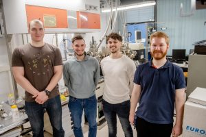
The team published its findings on 28 March 2022 in the journal Nature Communications. The study was conducted by a research group led by Nikolai Bart, Professor Andreas Wieck and Dr Arne Ludwig from the RUB Chair of Applied Solid State Physics. They worked in cooperation with the team led by Christian Dangel and Professor Jonathan Finley from the TUM Semiconductor Nanostructures and Quantum Systems research group and colleagues from the Universities of Copenhagen and Basel.
Producing quantum dots
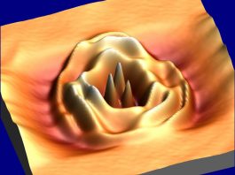
Quantum dots are narrowly defined areas in a semiconductor in which, for instance, a single electron can be confined. This can be manipulated from the outside, such as with light, so that information can be stored in the quantum dot. The researchers from Bochum created structures on a wafer made of a semiconductor material that is about the size of a beer coaster. The quantum dots have a diameter of only about 30 nanometres.
“Our quantum dots used to grow like mushrooms in the forest,” described Andreas Wieck. “We knew that they would emerge somewhere on the wafer, but not exactly where.”
Preliminary cultivation experiments
In a number of preliminary experiments, the team of researchers had already tried to influence the growth of the quantum dots on the wafer. The physicists had irradiated the wafer at individual points with focused ions, thus creating defects in the semiconductor crystal lattice. Acting like condensation nuclei, these defects provoked the growth of quantum dots.
“But just as cultivated mushrooms taste somewhat bland while forest mushrooms taste great, the quantum dots created in this way were not as high quality as the naturally grown quantum dots,” illustrated Andreas Wieck. They did not radiate light as perfectly as anticipated.
Therefore, the team proceeded with the naturally grown quantum dots. For the experiments, the wafer was cut into millimetre-small rectangles. They couldn’t analyse the whole wafer at once, because the vacuum chamber of the RUB apparatus was not large enough. However, the researchers observed that certain wafer rectangles contained many quantum dots, while others contained few. “At first, we didn’t notice any system behind it,” Andreas Wieck recalled.
High-quality quantum dots
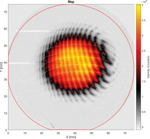
To explore the question in depth, the Bochum research team collaborated with their colleagues at the TUM, who had a measuring device with a larger sample chamber at their disposal at an early stage. During these analyses, the group discovered that there was a strange distribution of areas with high and low quantum dot densities on the wafer.
“The structures were strongly reminiscent of a moiré pattern that often occurs in digital images,” explained Arne Ludwig. “I soon hit on the idea that it must actually be a concentric pattern, i.e., rings, and that these could be seen in correlation to our crystal growth.” Measurements with higher resolution indeed showed that the density of quantum dots was distributed concentrically. Subsequently, the researchers confirmed that this arrangement was due to the manufacturing process.
In the first step, the wafer is coated with additional atomic layers. Due to the geometry of the coating system, this creates ring-shaped structures that have a complete atomic layer, i.e., where no atom is missing at any point in the layer.
Between the rings, similarly wide areas are formed that lack a complete atomic layer and thus have a rougher surface due to missing individual atoms. This has consequences for the growth of the quantum dots. “To stick with the image: rather than on a concreted surface, mushrooms prefer to grow on forest floor, i.e., on the rough spots on the wafer,” concluded Andreas Wieck.
The researchers optimised the coating process so that the rough areas appeared at regular intervals – of less than a millimetre – on the wafer and that the rings intersected. This resulted in an almost chessboard-like pattern with quantum dots of high quality, as demonstrated by the researchers from Basel and Copenhagen.