A team of researchers have uncovered a way to discover new graphene properties, despite these usually being difficult to observe.
The team, from the University of Amsterdam and New York University, have found a surprising way to solve this issue and discover new graphene properties.
Graphene is gaining a lot of attention as a strong two-dimensional material due to its unusual properties, which are very different from its three-dimensional ‘bulk’ counterparts. Graphene and many other two-dimensional materials are now researched intensely in the laboratory. Crucial to the unique properties of these materials are defects, locations where the crystal structure is not perfect. There, the ordered arrangement of the layer of atoms is disturbed, and the coordination of atoms changes locally.
The study, ‘Visualizing defect dynamics by assembling the colloidal graphene lattice,’ details the team’s intense study of graphene properties. It was published in the journal Nature Communications.
What is unique about graphene?
Graphene is the strongest of all two and three-dimensional materials. Moreover, it is exceptionally good at conducting heat and electrical currents, making it incredibly versatile. For these reasons, the discovery of graphene was awarded the Nobel Peace Prize in 2010.
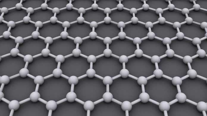
Graphene is made up of carbon atoms that each have three neighbours arranged in the well-known ‘honeycomb’ structure. This special structure enables graphene properties to be unique and mechanical.
Overcoming atom observation issues
Even though defects have been shown to be crucial for graphene properties, and because they are usually either present or added on purpose, little is known about how they form and evolve in time. This is because atoms are too small and move too quickly to be directly followed in real time.
In an effort to make the defects in graphene properties observable, the team of researchers found a way to build micrometre-size models of atomic graphene. To achieve this, they used so-called ‘patchy particles’.
These particles are large enough to be easily visible in a microscope yet small enough to reproduce many of the properties of actual atoms. They interact with the same coordination as atoms in graphene and form the same structure. The researchers built a model system and used it to obtain insight into defects, their formation, and evolution with time.
Building new graphene properties
Following the ‘honeycomb’ structure, the researchers used tiny particles made of polystyrene, decorated with three smaller patches of a material known as 3-(trimethoxysilyl)propyl (TPM).
The configuration of the TPM patches mimicked the coordination of carbon atoms in the graphene properties. The researchers then made the patches attractive so that the particles could form bonds, again in analogy with the carbon atoms in graphene.
After being left alone for a few hours, when observed under a microscope, the ‘mock carbon’ particles turned out to indeed arrange themselves into a honeycomb lattice.
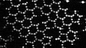
The researchers then looked more at defects in the model graphene lattice. The model worked, showing characteristic defect motifs also known from atomic graphene. Contrary to real graphene properties, the model’s direct observation and long formation time allowed the physicists to follow these defects from the start of their formation up to the integration into the lattice.
The new properties were unusual
The new look at the growth of the mock graphene properties immediately led to new knowledge about these two-dimensional structures. Unexpectedly, the researchers found that the most common type of defect already forms in the initial stages of growth when the lattice is not yet established.
Moreover, they observed how the lattice mismatch is then ‘repaired’ by another defect, leading to a stable defect configuration, which either remains or slowly heals further to a perfect lattice.
Thus, the model system not only allows to rebuild the graphene lattice on a larger scale for all kinds of applications, but the direct observations also allow insights into atomic dynamics in this class of materials. As defects are central to the properties of all atomically thin materials, these direct observations in model systems help further engineer the atomic counterparts, for example, for applications in ultra-lightweight materials and optical and electronic devices.