
2D materials possess unique application potential. To unravel it, fundamental science is as important as applied research.
With the isolation and characterisation of graphene 15 years ago, a new research area was born that focuses on ultrathin nanomaterials commonly referred to as two-dimensional (2D) materials. Due to quantum confinement effects, properties of 2D materials are distinct from their stacked three-dimensional counterparts. Today, more than 1500 structures have been identified that can exist in the 2D form. While graphene is moving towards commercial applications, many other 2D materials are completely unexplored.
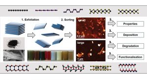
2D materials can be produced by bottom up or top down techniques. One strategy that has become increasingly popular is liquid phase exfoliation (LPE). In this process, a layered material (crystal or powder) is immersed in a suitable liquid medium and subjected to high-energy treatment such as sonication. The energy input overcomes the relatively weak interactions between the sheets, while the solvent adsorbs on the nanosheets thus preventing re-aggregation when appropriately chosen. With only little optimisation, this process can be applied to a whole host of bulk materials (examples of structure see Fig. 1).
Colloidally stable dispersions of nanosheets are obtained that can be further formulated into inks that can be solution-processed by a range of printing and deposition techniques. In its crudest form, LPE is a simple, yet scalable approach that makes these new materials accessible to researchers worldwide. Due to relatively high achievable masses (milligram to gram) even on the labscale, research activities in this area are driven by applications in diverse areas from nanocomposites, (opto)electronics and photonics to sensing and energy storage and conversion.
However, no matter what material or application, the full potential can only be exploited, when the entire process chain towards a given application is considered. The research in my group is dedicated to optimising processes on the nanoscale and mesoscale for solution processeable nanomaterials (Fig. 1), in particular 2D nanosheets, and understand fundamental, unifying principles and challenges across various classes of materials in a dialogue with researchers working on applications.
First steps in the process chain
LPE is not a very well controlled process and results in dispersions of nanosheets that are very polydisperse in lateral size and layer number. Since the size and in particular layer number determines the properties, a size selection in crucial. We recently developed an iterative centrifugation procedure termed liquid cascade centrifugation that can be widely applied to various materials and solvents to narrow the size distribution with only little wastage of material. Due to the importance of this point, we are constantly striving to develop new, innovative sorting concepts to achieve the control over nanosheet dimensions that is required. For example, the centrifugation procedures currently fail to isolate laterally large, yet thin sheets that would be of interest for example in polymer reinforcement.
Size and thickness distributions have to be quantified by statistical microscopy, for example atomic force microscopy. Even for experienced researchers in this area, this is extremely tedious and time consuming. For beginners, it is a nightmare scenario. It is therefore important to develop alternative methodologies to independently determine lateral size and layer number. This can be achieved spectroscopically, for example by absorbance/extinction, Raman or fluorescence spectroscopy. With knowledge of the size and thickness distribution, size-dependent changes to the spectroscopic properties can be linked to the size information to construct quantitative spectroscopic metrics. In particular, extinction/absorbance spectroscopy, which is a widely accessible tool, has proven powerful, as all 2D materials show similar changes to the spectral shape as function of size/thickness. Such metrics have now been developed for ~ 15 materials.
Studying size dependent properties of nanosheets in the liquid environment is interesting in its own right. Such investigations are typically carried out on micromechanically-exfoliated or CVD-grown materials. However, when analysing individual nanosheets on a substrate, local impurities, defects and strain have an impact on the optical properties. In the liquid environment, an ensemble of sheets is measured in a homogeneous environment (the solvent) so that such local variations are averaged out and the optical properties can be quite intrinsic (i.e. comparable to free-standing high quality nanosheets). It is therefore of great interest to compare the results on high quality liquid-exfoliated nanosheets to other sample types in particular in the case of less common layered crystals.
Achieving good control of both size and inherent properties in dispersion is an important step. However, it is often equally important to maintain the nanosheet properties also in thin films, where reaggregation occurs. Typically, nanosheet networks are produced from vacuum filtration, spraying or printing. While such porous networks have proven useful for electrocatalytic applications or in all-printed, all nanosheet network transistors, this is not always beneficial. In addition, such porous networks do not allow a defined control of the interface which is required for understanding processes associated with the nanosheet surface. To this end, we are currently developing strategies to deposit individual layers of nanosheets. We can use the photoluminescence of monolayered transition metal dichalcogenides as indicator, whether monolayer properties are retained in thin films and use this observable to optimise the deposition processes. While this is not of immediate technological relevance, it is important to have access to such sample types, e.g. to test application potential in optical or optoelectronic applications.
Little is known about the environmental stability of novel 2D materials. It is well accepted that graphene and h-BN are rather inert, while other materials such as black phosphorus or NbSe2 are known to rapidly oxidise in air. It is therefore crucial to assess the environmental stability of new, more exotic 2D materials. The understanding of the optical spectra of the nanosheets gives the unique possibility to monitor degradation kinetics in various liquid environments by following the spectral evolution as function of time and temperature. In this way, the activation energies of the degradation can be determined. This procedure can be applied to a range of materials with different lateral sizes to gain insights in the degradation mechanism. For example, size selection allows us to test whether the reaction occurs from edge inwards or on the basal plane. Importantly, such experiments are also an ideal reference to develop defect passivation by functionalisation.
Functionalisation
Last but not least, being a chemist by training, I have great interest in modifying the nanosheet surface area- both on edge and basal plane. Functionalisation of 2D materials will play a key role for interfacing the materials with other compound classes and to potentially tune and tailor properties (Fig. 2). Thus far, we have developed three different functionalisation routes based on redox chemistry, coordination chemistry and diazonium salt chemistry, respectively, that can be applied to either liquid-exfoliated transition metal dichalcogenides or nanosheets after chemical exfoliation which are negatively charged and thus metallic rather than semiconducting.
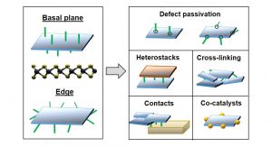
This shows that this class of materials is significantly less inert than previously thought. Currently, our work focuses on defect passivation which greatly improves the environmental stability of the nanosheets. We hope to develop strategies to controllably modify edge and/or basal plane selectively. This would give the opportunity to build vertical inorganic-organic-inorganic heterostacks or cross-link nanosheets in a film to, for example, improve charge transport. Functionalisation can also be of potential interest for contact doping or to construct hybrids with other nanomaterials, for example nanoparticles as co-catalysts. With proof of concept functionalisation sequences in place, we can now begin to explore such opportunities.
Claudia Backes
Junior Research Group Leader
Heidelberg University
+49 6221 54 5378
backes@uni-heidelberg.de


