Business Finland’s eBook explores Finland’s ‘Chips from the North’ strategy and its impact on the semiconductor industry, highlighting Finnish expertise in microelectronics, photonics, and quantum technologies, which drive sustainable growth and strengthen Europe’s technological resilience.
Finland’s Chips from the North strategy
The Finnish semiconductor industry plays a strategically important role in the European technology landscape. Finland’s strengths may not lie in high-volume production of semiconductors, but the research, development, and production of high-quality, specialised microelectronics and photonics are natural to Finland’s ecosystem.
Specialisation has been the key to success for Finland, which has a strong background in System-on-Chip (SoC) design – a legacy that dates back to Nokia’s expertise in telecommunications circuit design. Nokia’s extensive technological advances have strengthened Finland’s microelectronics development in several areas. Today, its extensive specialisation has made Finland a research and development hub that attracts major global players.
Finland’s recent ‘Chips from the North’ industry strategy is a comprehensive national initiative aimed at transforming the country into a leading centre for semiconductor and microelectronics innovation in Europe. With the global semiconductor landscape undergoing major shifts due to technological advancement, geopolitical tensions, and supply chain vulnerabilities, Finland sees an opportunity to play a central role in Europe’s response. This strategy outlines a vision for strong, sustainable growth, driven by deep technological expertise and a collaborative ecosystem.
The country aims to more than triple the size of its semiconductor industry by 2035, targeting annual growth rates of over 10%. Revenue from the sector is projected to increase to €5-6bn, while the workforce is expected to double to around 20,000 employees. This growth is supported by Finland’s robust foundation in electronics and telecommunications technologies, largely inherited from global leaders such as Nokia, and a thriving ecosystem of deep tech startups that have emerged over the past decade.
The strategy identifies six key areas where Finland holds significant competitive advantages. These include chip design, microelectromechanical (MEMS) systems and sensor innovations, photonics, quantum technologies, advanced semiconductor materials, and sustainable manufacturing processes. Each area is backed by world-class research institutions and a strong education system, as well as existing companies that specialise in advanced technologies such as Atomic Layer Deposition (ALD), optical sensors, and quantum computing.
Finland offers a highly attractive business environment for both R&D-intensive businesses and manufacturing, offering an ecosystem that combines a highly skilled workforce, competitive labour costs and an active business environment. Good examples of companies that have been very successful in Finland include MEMS sensor manufacturers Murata and Kyocera, as well as Okmetic, a supplier of silicon wafers. Picosun/Applied Materials, Beneq, and ASM, all of which are leading manufacturers of atomic layer deposition (ALD) equipment for the semiconductor industry, have found Finland to be a great place for product development.
In the research field, Finnish universities — especially Aalto University, Tampere University, the University of Oulu, the University of Eastern Finland, the University of Turku, and VTT (the technical research centre of Finland) — are internationally renowned for their research in photonics and microelectronics. Achieving the goals outlined in the Chips from the North strategy will require targeted investments in talent development, research and development, and infrastructure. Finland is already making progress through public funding or EU-aligned pilot projects and the upcoming national Chips Competence Centre. Success will depend on close cooperation among industry players, academic institutions, and government agencies, with organisations like Business Finland and Technology Industries of Finland playing a key role in coordinating national and EU-level engagement.
In summary, Finland’s semiconductor strategy presents a timely and ambitious plan to scale innovation, support economic growth, and make a meaningful contribution to Europe’s technological sovereignty. With the right investments and collaborations, Finland is poised to become a cornerstone of the continent’s renewed semiconductor capabilities.
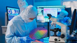
The Finnish Chips Competence Centre: A northern powerhouse in Europe’s Chip Strategy
How the Finnish Chips Competence Centre is reshaping Europe’s semiconductor future
In early 2025, Finland quietly took a bold step into the future of microelectronics. A new type of national alliance emerged: the Finnish Chips Competence Centre (FiCCC). Backed by both Chips JU and Business Finland, FiCCC is more than just a support service for chip design. It’s a gateway. A signal that Finland intends to be more than a player – Aiming to be a force in Europe’s semiconductor race.
Why now? The world is currently experiencing a semiconductor supercycle. The global market size is expected to surpass €1tr by 2030, and Europe aims to capture a larger share of the market. Through the EU Chips Act, Europe is investing in pilot lines, design platforms, and 27 national competence centres. FiCCC is Finland’s entry into this strategic network.
A northern hub with reach
FiCCC was built on a clear mission: strengthen Finland’s chip capabilities, plug them into Europe, and support companies across the spectrum, especially startups and SMEs. Its structure mirrors Finland itself: distributed, tech-savvy, and deeply collaborative.
Spanning across four regions, the four partners are:
- Tamlink in Tampere
- Kvanttinova Oy in Espoo
- BusinessOulu in Oulu
- Photonics Finland in Joensuu
Each brings unique strengths, from high-performance SoC design and quantum technology to sensors, advanced photonics, and RF systems. All are united by a simple idea: Finland’s edge lies in its ability to collaborate across silos.
What does FiCCC do?
At its core, FiCCC exists to make advanced chip development more accessible. This means:
- Helping SMEs and startups jump into IC design and advanced manufacturing with expert support and access to tools like the upcoming EU Design Platform.
- Bridging research and industry, often through co-innovation projects.
- Offering guidance to pilot lines and feeding their capabilities back to Finnish companies.
- Building training pipelines that match what real-world companies need.
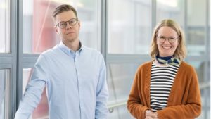
“We want to lower the threshold for companies to get involved in semiconductors,” explained Elina Mielityinen, FiCCC Coordinator. “If you have an idea and need guidance, we’re here to help open the right doors.”
Real progress, fast
Even in its first weeks of official operation, FiCCC was moving quickly. It established ties with Nordic peers, plugged into several EU working groups, and began mapping startup needs and training gaps. Companies from fields as diverse as Complex SoC design, cryptography IP, and wireless RF have already shown interest.
In Tampere, the WBG pilot line partner, SiPFAB, is gearing up to prototype system-in-package solutions. In Espoo, Kvanttinova is scaling up jointly with VTT as the hosting site of several EU pilot lines. In Oulu, FiCCC is already supporting co-innovation proposals that link wireless heritage with next-generation chip design.
Tomi Salo, Co-Creation Manager at Kvanttinova, stated: “We cover the journey from design to early-stage production. And we do it by co-creating with the companies themselves.”

From Finland to Europe and back again
FiCCC is Finland’s official member in the European Network of Chips Competence Centres (ENCCC). That matters. It gives Finnish companies access to Europe-wide prototyping and design services, while allowing Finnish strengths (like ALD processes, advanced sensors, and photonics) to feed back into the European innovation loop.
Startups like Xiphera (crypto-IP), CoreHW (RF), and Winse Power (optoelectronics) are already part of the broader network. FiCCC helps these companies find funding, partnerships, and infrastructure, and ensures their breakthroughs contribute to Europe’s semiconductor future.
Looking ahead: From chips to sovereignty
FiCCC isn’t just about microchips. It’s about enabling Europe to build its digital foundations within its own borders. It’s about letting a Finnish startup design and test a chip without relying on services worldwide. It’s about sovereignty, resilience, and industrial competitiveness.
From discovery to impact: Industrialising innovation for a sustainable future
Chips – the backbone of semiconductors, microelectronics, and quantum computing – are among the critical technologies shaping our future.
Kvanttinova is an ecosystem for players in the fascinating field of chips and chip-based systems, which catalyses innovation and brings people and companies together, all while hosting a fun and beneficial community. The organisation facilitating the ecosystem, Kvanttinova Ltd., is a joint initiative co-founded by VTT, Aalto University, the City of Espoo, and Enter Espoo, and is supported by the Finnish semiconductor industry.
In the Kvanttinova ecosystem, Aalto University’s education and research excellence connect with VTT’s strong expertise in the specialised microelectronics processes and quantum technology. This collaboration between education, applied research, and the business landscape forms the heart of Espoo’s innovation ecosystem, and thus Kvanttinova’s.

Micronova, a multi-user R&D piloting environment in Otaniemi, has brought Finland groundbreaking technology companies, such as ElFys, Chipmetrics, and SemiQon, and attracted companies to further develop their innovations in the vicinity, including Dispelix. This success is about to be scaled up with the Kvanttinova ecosystem.
Ecosystem for players in microelectronics and quantum technology
The Kvanttinova ecosystem welcomes all aspects of microelectronics, with the goal of creating new business, boosting Finnish competitiveness, and strengthening Finland’s position as an invaluable asset to the European future. The basis of the ecosystem is a sense of togetherness among the different actors in our community, who attend various events, co-create in organised or spontaneous encounters, and work together on common projects, some even in shared facilities.
By bringing together innovative circuit design and advanced materials, unforeseen devices and products are created in the Kvanttinova ecosystem. This unique environment enables the research and development of new products, from design to proof-of-concept validation. Application technologies include 6G, healthcare and medical, aerospace and defence, as well as AI and of course, quantum computing.
Local collaboration, global impact
A recent milestone, underscoring the strength of Espoo’s innovation community in bringing together world-leading expertise, talent, and infrastructure, is the announcement that IQM, a spinoff from Aalto University and VTT, will deliver a 300-qubit superconducting quantum computer to VTT by 2027. VTT’s procurement includes an innovation partnership with IQM in technology development, application and services. Their previous co-development success was Europe’s first 50-qubit superconducting quantum computer, launched in 2025. Thus, the local value chain further strengthens Finland’s position in the global quantum technology landscape.
Ecosystem’s infrastructure
The core infrastructure of the Kvanttinova ecosystem is the VTT-hosted, shared-use Micronova R&D piloting environment, along with upcoming new facilities that VTT and companies will occupy with their own R&D and production sites. VTT’s piloting environment will include state-of-the-art equipment for chip development and pilot production on 200 mm and 300 mm wafers.
The focus technologies include quantum technologies, post-CMOS processing, MEMS, RF technologies, integrated photonics, and material development. VTT is part of the Chip JU pilot lines FAMES, APECS, NanoIC, and PIXEurope.
Reinventing the ecosystem – together we make the difference
As important as the fascinating new facilities and infrastructure are, we are even more excited to facilitate our ecosystem members, both old and new, to meet, learn, and co-create, leading to growth for us all. It’s well known that we are stronger together. Kvanttinova is eager to grow into a leading ecosystem for chip-based innovations, providing both the environment and support to scale science into business.
To support the growth of our community, Kvanttinova Ltd. collaborates with educational institutions at all levels to address the common challenge of finding the skills and talent needed to meet the ambitious targets of the microelectronics industry. We are committed to promoting the field to students by demonstrating its importance to them and strengthening their understanding of career opportunities. Going even deeper, we aim to support the educational institutions in developing novel educational concepts for upskilling and reskilling of the existing workforce.
The momentum is now
We strongly believe that the integration of chips and systems, enabling an increase in the level of digitalisation in products and offerings across any industrial vertical, leads to a significant increase in the competitiveness of companies. Doing this sustainably means a vital and flourishing future for the entire planet. Promoting the benefits of digitalisation while raising awareness of the services available in our ecosystem for chip design and processing will attract new users and customers to service providers and chip-producing companies.
Kvanttinova Ltd. and its partners in the Finnish Chips Competence Centre (FiCCC) can assist in finding R&D consortia and funding through our connections.
We welcome all interested parties to collaborate in our ecosystem, Kvanttinova.