VUO-IC as Finland’s gateway to making complex SoCs a reality.
Europe’s ambition to strengthen its semiconductor and electronics value chains has been clearly articulated through the European Chips Act. Beyond headline investments in manufacturing capacity, pilot lines, and research infrastructures, the Chips Act recognises a more subtle but equally critical challenge: turning ideas, architectures, and system concepts into functional devices on silicon.
For many European companies–especially SMEs, deep-tech startups, and system houses–the primary bottleneck is not creativity, but access to design execution capability. Advanced SoC development, mixed-signal integration, RF, photonics, and emerging More-than-Moore technologies require specialised workflows, reusable IP, experienced teams, and early access to prototyping paths. Building this capability independently is time-consuming, capital-intensive, and often takes the focus away from what’s important for business.
To address this gap, the Chips Act introduced Design Enablement Teams (DETs) as part of the broader European Chip Design Platform (EuroCDP). DETs act as structured, application-oriented entry points into Europe’s semiconductor ecosystem. Their role is not to replace commercial design houses or academic research, but to connect users to real design execution, reduce friction between organisations, and significantly shorten the path from concept to demonstrator.
Within this European network, VUO-IC represents Finland’s national Design Enablement Team–bringing together universities, research and technology organisations, and commercial design houses into a single, coordinated delivery model.
What Design Enablement Teams actually do
At their core, DETs are built around a pragmatic principle: enables users to deliver chips, not just designs. This distinguishes DETs from advisory services, funding instruments, or purely academic support structures.
A Design Enablement Team typically:
- Provides a single entry point for users with chip-related ambitions
- Assesses technical feasibility and design scope early
- Connects users to the right combination of design, IP, and infrastructure resources
- Supports execution through traceable workflows
- Plans the route to prototypes and first silicon, learning from the outset
Crucially, DETs are structured to operate across organisational boundaries. They translate high-level policy goals – such as European technological sovereignty – into concrete, case-based support for companies that need to build hardware products under real commercial constraints.
VUO-IC: Finland’s Design Enablement Team
VUO-IC is Finland’s EuroCDP Design Enablement Team, designed to help users deliver real chips – from system architecture and design implementation to prototypes and first silicon learning – through a coordinated service model that combines university-scale SoC capability, industrial design execution, and national prototyping access.
What differentiates VUO-IC within the European DET landscape is its readiness for complex digital SoC delivery. Rather than focusing only on small demonstrators or isolated IP blocks, VUO-IC is structured to support large-scale, system-level designs where complexity is often the main barrier to progress.
This capability is anchored by Tampere University, which provides a production-grade design environment and workflows suitable for complex SoCs. Beyond tools, the university contributes SoC templates, reusable building blocks, and low-level software know-how–elements that are often overlooked but are essential for avoiding a ‘from scratch’ approach in advanced designs. In practice, this can dramatically shorten the time needed to reach a first functional demonstrator.
Industrial-grade execution is provided by CoreHW and VLSI Solution, two established Finnish design houses. CoreHW brings deep RF and mixed-signal expertise together with a large, validated IP base, while VLSI Solution contributes full-stack ASIC delivery experience from design through production, demonstrated through long-term commercial track records and high-volume shipments. Their involvement ensures that designs developed within VUO-IC are aligned with real manufacturing and productisation requirements from the outset.
VTT complements this foundation with advanced RTO capabilities in RF and mmWave technologies, photonics, and quantum and cryogenic CMOS. VTT also plays a key role as an interface to prototyping infrastructures, ensuring that emerging and cross-domain technologies can be integrated into realistic chip development paths.
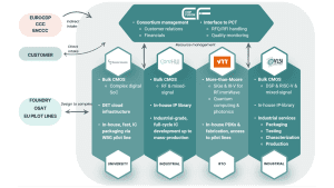
Coordination and orchestration are provided by Chip Fusion, which manages intake, case routing, and delivery oversight. Through its leadership role in Finland’s semiconductor coordination structures, Chip Fusion also connects VUO-IC to the wider national ecosystem, ensuring that users do not need to navigate complex institutional landscapes on their own.
A service model built for execution
VUO-IC operates through a structured, case-based service model rather than open-ended consulting. This is an important distinction: users engage with defined service steps across the chip lifecycle, from early feasibility assessment to tape-out readiness and prototyping planning.

All engagements begin with a single front door, managed by Chip Fusion. Each case is triaged and routed to the appropriate execution teams with clear ownership, preventing projects from stalling between organisations. Delivery follows a documented workflow–scoping, activation, delivery, and closure–where assumptions, constraints, and decisions are explicitly captured and handed over.
A defining feature of the VUO-IC model is that the prototype path is planned early. If a user targets silicon, considerations related to MPW access, packaging, testing, interfaces, and bring-up are addressed from the beginning rather than after design completion. This reduces late-stage surprises and increases the likelihood that ‘design complete’ translates into working device on silicon.
When cases require additional infrastructure–such as pilot lines, specialised packaging or testing, or domain-specific expertise–VUO-IC orchestrates access through its consortium and Finland’s broader ecosystem, presenting users with a coordinated path instead of fragmented contacts.
Why this matters for companies
VUO-IC offers more than technical support – it provides a credible shortcut into the European electronics value chain.
First, it lowers the threshold for engaging in complex chip development. Companies no longer need to assemble complete SoC capability internally before taking their first steps. By leveraging existing templates, IP, workflows, and experienced teams, they can focus on differentiation and system value rather than infrastructure building.
Second, it bridges the gap between research and industrialisation. With universities, RTOs, and commercial design houses working as one delivery team, projects are less likely to fall into the common trap of being ‘too academic for industry’ or ‘too rushed for robustness.’
Third, it enables mixed technology domain innovation. Many future products – whether in wireless, sensing, photonics, or quantum-adjacent systems – do not fit neatly into a single technology silo. VUO-IC’s ability to span digital SoC, RF, mmWave, photonics, and More-than-Moore technologies within one Design Enablement Team is particularly valuable in this context.
Finally, participation in VUO-IC embeds companies directly into European design and prototyping flows aligned with the Chips Act. This visibility and integration are essential if companies seek to become meaningful contributors to the European electronics ecosystem rather than a peripheral technology provider.
Towards an integral role in Europe’s future value chains
Design Enablement Teams represent a shift in how Europe approaches semiconductor competitiveness: from isolated excellence to coordinated capability building. VUO-IC demonstrates how this concept can be implemented at the national level without fragmentation, duplication, or excessive bureaucracy.
By combining production-grade academic environments, proven industrial execution, advanced RTO capabilities, and structured orchestration, VUO-IC turns policy intent into practical delivery. For Finnish companies, it offers a tangible pathway from idea to functional device on silicon. For Europe, it strengthens the connective tissue between design, prototyping, and future manufacturing.
As the European electronics value chain evolves – towards greater complexity, heterogeneity, and system integration – such models will be increasingly central. In this sense, VUO-IC is not only Finland’s Design Enablement Team, but also a blueprint for how smaller, highly specialised ecosystems can play a decisive role in Europe’s semiconductor future.
VUO-IC value proposition for users
A proven shortcut to complex SoCs: You don’t need to build everything from zero. We bring SoC templates, reusable blocks, and the practical know-how (including low-level SW interfaces) that typically takes years to assemble.
Industrial-grade execution, not academic guidance: Two commercial design houses complement the university/RTO strengths, with validated IP libraries and experience delivering chips that ship.
One team across digital + RF + More-than-Moore: Digital SoC, RF/mixed-signal, RF/mmWave, photonics, and quantum-related paths are covered inside one DET, so mixed-domain projects don’t get fragmented.
A clear route to prototypes and first silicon learning: We plan MPW, packaging, and bring-up as part of the same delivery flow – so ‘design complete’ becomes ‘working silicon’.
Single intake, clear routing, traceable delivery: Chip Fusion runs a practical triage and orchestration model, so users know who does what, what is needed next, and how progress is tracked.
Partners:
Please Note: This is a Commercial Profile

This work is licensed under Creative Commons Attribution-NonCommercial-NoDerivatives 4.0 International.
Please note, this article will also appear in the 25th edition of our quarterly publication.