
The NanoIC pilot line has the ambition to become the world’s specialised R&D pilot line on beyond semiconductor technology.
With the aim to support the European Chips Act’s vision to reinforce Europe’s leadership in the global semiconductor ecosystem and drive innovation in critical markets like computing, communication, mobility, energy, and health. Serving as a vital bridge between cutting-edge research and commercial applications, the NanoIC pilot line is central to consolidating Europe’s position at the forefront of semiconductor innovation and competitiveness.
To bridge the gap between research innovation and commercialisation in the semiconductor industry, a robust lab-to-fab conduit is essential. The NanoIC pilot line fosters innovation in computing system architectures by maturing specific semiconductor technologies. The goal is to enable European companies to further lead in semiconductor innovation.
Specifically, the NanoIC pilot line provides a beyond 2nm system-on-chip (SoC) pilot line for the development and maturation of selected advanced logic, memory, and interconnect technologies. The project focuses on large-scale capacity building, especially in imec’s cleanroom in Leuven (Belgium), joint R&D, maturation of advanced technologies towards prototyping, and innovation support, providing the entire semiconductor ecosystem access to these advanced technologies. Participants can engage with the NanoIC pilot line in ways that best suit their specific needs and innovation goals, regardless of their role in the value chain. This will allow early insights into the emerging fields and support Europe to maintain its competitiveness across the entire semiconductor value chain: from materials, equipment, processes and devices to designs and systems.
NanoIC consortium
The NanoIC pilot line project consortium is led by imec, alongside CEA-Leti in France, Fraunhofer-Gesellschaft (FhG) in Germany, VTT Technical Research Center in Finland, Tyndall National Institute in Ireland, and the Center for Surface Science and Nanotechnology of the University Politehnica of Bucharest in Romania.It is supported by the Flemish Government, other participating states, and the Chips Joint Undertaking. All partners together strive to make the implementation of the pilot line a success.
Building blocks of future compute systems
Nanosheet class of logic devices are anticipated to drive scaling and performance through three more generations (N2, A14, A10). Complementary field effect transistor (CFET) architectures are currently projected to be introduced around 2031 at the A7 node, representing a major inflection point in CMOS device design. Progression in this field demands extensive research into new materials, process modules, equipment, and advanced patterning capabilities, for which high numerical aperture extreme ultraviolet (high NA EUV) lithography comes into play.
Memory innovations are focusing on novel magnetic memories, more specifically spin orbit torque-magnetic random access memory (SOT-MRAM) and embedded Dynamic Random Access Memory (eDRAM). For the latter, an alternative 2T0C configuration is developed, including the exploration of semiconductors with wide bandgaps, such as semiconducting oxides like indium-gallium-zinc-oxide or 2D transition metal dichalcogenides, which are considered promising alternative channel materials. In parallel, developing a 3D memory platform to explore future novel memory options – to augment SRAM and DRAM – is essential to address memory capacity and memory bandwidth challenges from new workloads.
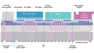
To integrate different dies into systems, 2nm and beyond advanced electrical and optical interconnects are required. To further advance electrical interconnects, 3D heterogeneous integration, like die-to-wafer (D2W) hybrid bonding techniques, will be enabled. To electrically connect dies side-by-side and enable 2.5D chiplet integration on a low-cost interposer platform, the NanoIC pilot line will target lines under 2µm, offering fine-pitch redistribution layer (FP RDL) technology based on copper line and via, embedded in polymers.
The above-mentioned leading-edge logic, memory, and interconnect technologies, defined at industry-relevant dimensions, are at the heart of the NanoIC pilot line. Their enablement requires evaluation of new processes and materials, demands a tighter process control, and relies on a versatile set of validation routes. Setting up relevant process modules requires investment in entirely new capabilities in processing and metrology tools. These modules are the building blocks for the baseline flows and are prone to continuous improvements, ensuring maturation, increasing the speed of learning and pushing towards higher TRL. Stabilised baseline flows represent R&D collaboration opportunities exemplified by materials and equipment vendors to remain at the forefront of innovation.
Lowering the barriers to advanced chip designs with advanced PDKs
To help European designers, in academia and industry, to explore these findings in logic, memory, and interconnect technologies, the NanoIC pilot line provides early access to advanced process design kits (PDKs).
These PDKs are comprehensive toolsets that provide designers with the predictive models, cell libraries, and system-level integration resources, enabling accurate simulation and validation of integrated circuits for advanced technology nodes. By making these hands-on kits available, circuit designers can explore upcoming chip architectures, address complex design challenges and support innovation in beyond 2nm nodes.
Specifically, the NanoIC pilot line offers two complementary PDKs: pathfinding PDKs for early design exploration in beyond-state-of-the-art lC technologies, and system exploration PDKs to pave the way for hardware prototyping and system-level innovation.
These PDKs are being released throughout the project and include multiple versions of the N2 pathfinding PDK, including releases in A14 and A7 logic PDKs. Memory PDKs are based upon the progress in eDRAM and SOT-MRAM, while for advanced interconnect solutions, they can be explored through RDL, silicon interposer and D2W hybrid bonding.
Driving innovation in Europe
The NanoIC pilot line provides flexible access to advanced logic, memory, and interconnect technologies for the entire semiconductor ecosystem. Companies, research institutes, start-ups, and universities can collaborate according to their innovation needs.
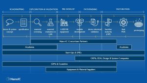
Integrated device manufacturers and foundries can leverage the baselines to explore new modules and performance enhancement options. Equipment and materials suppliers, both European and global, are invited to collaborate to enable the advanced baselines to test and refine new tools and processes. Furthermore, start-ups, universities, and design companies have access to the pathfinding PDK for early design exploration of future nodes and system exploration PDKs for hardware prototyping and system-level innovation. Moreover, the NanoIC pilot line is committed to nurturing the next generation of semiconductor experts. Partnering with the EU Competence Centers, we provide classroom and virtual courses on beyond 2nm technologies, from semiconductor materials to SoC design. Our hands-on internships and learning programmes offer students real-world experience, while our industry-oriented trainings prepare Bachelor’s, Master’s and PhD students for future challenges. Through expert courses, technical training, and immersive bootcamps, the NanoIC pilot line is building a skilled workforce to propel the European semiconductor industry forward.

In summary, the NanoIC pilot line is strategically positioned to bridge the gap between cutting-edge research and commercial applications in the semiconductor industry. The project underscores Europe’s commitment to innovation, competitiveness, and sustainable growth in an increasingly digital world. By advancing technologies and fostering collaboration, the project aims to consolidate Europe’s leadership in the global semiconductor market.
Disclaimer
The acquisition and operation of the NanoIC pilot line are jointly funded by the Chips Joint Undertaking, through the European Union’s Digital Europe (101183266) and Horizon Europe programmes (101183277), as well as by the participating states Belgium (Flanders), France, Germany, Finland, Ireland and Romania. For more information, visit nanoic-project.eu.
This article is based on the comment published in Nature Reviews Electrical Engineering (Volume 1 | December 2024 | 764–765 | 764).
Please note, this article will also appear in the 24th edition of our quarterly publication.