Researchers at Nagoya University in Japan have used Artificial Intelligence to discover a new method for understanding small defects called dislocations in polycrystalline materials.
Polycrystalline materials are widely used in information equipment, solar cells, and electronic devices, which can reduce the efficiency of such devices.
The research, ‘Multicrystalline Informatics Applied to Multicrystalline Silicon for Unraveling the Microscopic Root Cause of Dislocation Generation,’ was published in Advanced Materials.
Polycrystalline materials are commonly used, but they pose a problem
Almost every device that we use in our modern lives has a polycrystal component – from smartphones to computers and the metals and ceramics in cars.
Despite this, polycrystalline materials are tough to utilise because of their complex structures. Along with their composition, the performance of a polycrystalline material is affected by its complex microstructure, dislocations, and impurities.
A major problem with using polycrystals in industry is the formation of tiny crystal defects caused by stress and temperature changes.
These are known as dislocations and can disrupt the regular arrangement of atoms in the lattice, affecting electrical conduction and overall performance.
It is important to understand the formation of these dislocations to reduce the chances of failure in devices that use polycrystalline materials.
How did the research aim to overcome these issues?
The research on polycrystalline materials was led by Professor Noritaka Usami and included Lecturer Tatsuya Yokoi and Associate Professor Hiroaki Kudo and collaborators.
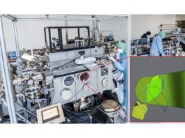
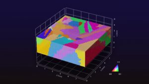
They used a new Artificial Intelligence to analyse image data of a material widely used in solar panels, called polycrystalline silicon. The AI created a 3D model in virtual space, helping the team to identify the areas where dislocation clusters were affecting the performance of polycrystalline materials.
After identifying the areas of the dislocation clusters, the researchers used electron microscopy and theoretical calculations to understand how these areas formed.
They revealed stress distribution in the crystal lattice and found staircase-like structures at the boundaries between the crystal grains. These structures appear to cause dislocations during crystal growth.
“We found a special nanostructure in the crystals associated with dislocations in polycrystalline structures,” Usami said.
Along with its practical implications, this study may also have important implications for crystal growth and deformation science. The Haasen-Alexander-Sumino (HAS) model is an influential theoretical framework used to understand the behaviour of dislocations in materials.
However, Usami believes that they have discovered dislocations that the Haasen-Alexander-Sumino model missed.
A surprising discovery
The team were surprised when they calculated the arrangement of the atoms in polycrystalline materials, finding unexpectedly large tensile bond strains along the edge of the staircase-like structures that triggered dislocation generation.
Usami explained: “As experts who have been studying this for years, we were amazed and excited to finally see proof of the presence of dislocations in these structures. It suggests that we can control the formation of dislocation clusters by controlling the direction in which the boundary spreads.”
He added: “By extracting and analysing the nanoscale regions through polycrystalline materials informatics, which combines experiment, theory, and AI, we made this clarification of phenomena in complex polycrystalline materials possible for the first time.”
Overall, the research illuminates the path towards establishing universal guidelines for high-performance materials and is expected to contribute to the creation of innovative polycrystalline materials.