Lilei Ye, Business Developer for electronics applications for the Graphene Flagship, explains the state of play for graphene in electronics, and the challenges that lie ahead.
Moore’s Law states that, every two years, the number of transistors on a microchip doubles, while the cost of computers is halved. Today, however, semiconductor technology is reaching its molecular limits, opening up a gap in the market for new approaches. Two-dimensional (2D) materials, including graphene, offer one way to unlock the next generation of electronics, and research for this advancement is underway in the Graphene Flagship.
The physical properties of 2D and layered materials like graphene offer immense potential for the electronics sector, promising faster, smaller and more powerful devices. These materials have the potential to stretch the boundaries of what we currently believe electronics should do or be. Think futuristic products like smart textiles that keep you warm or cool in line with the weather, brain implants that monitor and treat health conditions, or circuits that can be printed on any surface, even paper. All this is possible with graphene.
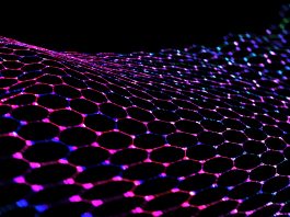
Just a single carbon atom thick, yet stronger than steel and harder than diamond, it is the physical properties of graphene that make it such an exciting prospect for electronics. Most importantly, graphene is an incredible conductor – 12 times more so than copper. In addition, graphene is mechanically flexible, chemically stable, disperses heat and is lighter than aluminium.
There are numerous applications for 2D materials in electronics, including detectors, modulators, imagers, sensors and transceivers, many of which are being researched by partner research institutions and companies in the Graphene Flagship; the pan-European research project with the aim of taking graphene out of the lab and into society.
To exploit the potential of 2D electronics, however, we must be able to mass manufacture them – a notoriously difficult step.
Developing manufacturing techniques
The main challenge with manufacturing 2D electronics is the transfer step. Graphene is commonly mass produced using the chemical vapour deposition (CVD) method. Here, layers of graphene are deposited on a metal or insulating layer, or growth substrate. To be integrated into electronics, the graphene must be moved from the growth substrate to the desired component. However, current methods are either not compatible with high-volume manufacturing, or result in significant degradation of the 2D material and its electronic properties.
Arne Quellmalz, Researcher at the Graphene Flagship, Associate Member KTH and lead author of the paper, said: “There is always this critical step of transferring from a special growth substrate to the final substrate on which you build sensors or components.
“You might want to combine a graphene photodetector for optical on-chip communication with silicon read-out electronics, but the growth temperatures of those materials are too high, so you cannot do this directly on the device substrate.”
However, mass manufacturing methods for 2D electronics are getting closer to reality. A team of Graphene Flagship researchers in Sweden and Germany have published a new technique, which effectively transfers 2D materials from their growth substrate to the desired electronics, using existing tools and methods used in semiconductor manufacturing.
Essentially, the researchers glued two wafers together using a resin made of the commonly used dielectric material bisbenzocyclobutene (BCB). The researchers heat the resin until it becomes viscous then press the 2D material against it. When cooled to room temperature, the resin becomes a solid layer, providing a stable connection between the wafer and the 2D material. The process can be repeated to stack or layer further 2D material onto the component.
Professor Max Lemme, from Graphene Flagship partners AMO GmbH and RWTH Aachen University, said: “Our transfer method is, in principle, applicable to any 2D material, independent of the size and the type of growth substrate.
“And, since it relies only on tools and methods that are already common in the semiconductor industry, it could substantially accelerate the appearance on the market of a new generation of devices where 2D materials are integrated on top of conventional integrated circuits or microsystems.”
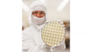
To further develop manufacturing methods and therefore realise the commercial potential of graphene-based electronics, the Graphene Flagship has launched a new project, the 2D-Experimental Pilot Line (2D-EPL).
Graphene and the semiconductor shortage
The 2D-EPL has been created to establish a sustainable European ecosystem for graphene electronics – a world-first graphene foundry working to integrate graphene and other layered materials into semiconductor platforms.
The project also looks to offer a solution to the most pressing challenge facing the semiconductor sector. The world is currently experiencing a global shortage of semiconductors, which is expected to last until the end of 2023. This shortage has a significant impact on the production of high-tech products around the world, affecting everything from cars to personal computers and mobile phones. In fact, the automotive industry alone is expected to lose an estimated $210bn in revenue due to this issue. The problem is so severe, in fact, that the European Commission has announced the European Chips Act, adding €15bn to an existing €30bn in public investments to build new infrastructure to address the shortage.
So, what caused this shortage? Commonly cited factors include scarcity of metals usually used in electronics manufacturing, reduced output from producers, higher than expected demand, and supply chain disruption caused by the pandemic and harsh weather conditions. Plus, it takes a long time for semiconductor manufacturers to increase their output.
Another challenge facing the semiconductor industry is performance of the components themselves. Silicon is used extensively across the semiconductor industry but is increasingly reaching the limits of its performance. This is particularly apparent in the light of the increased speed, reduced latency and improved light detection demands of new technologies like the Internet of Things (IoT), robotics, Artificial Intelligence (AI), self-driving cars and 5G and 6G enabled phones.
The 2D-EPL will pioneer the development of graphene-integrated wafers for prototype electronics, sensors and photonic devices, utilising the properties of graphene to create devices that surpass the performance of silicon equivalents. It will also offer comprehensive prototyping services to companies, research centres and academics, to foster innovation around 2D-electronics. At the same time, the 2D-EPL will investigate the optimum manufacturing methods to produce these wafers, collaborating with European partners the whole way along the value chain.
Cedric Huyghebaert, Technical Leader of the 2D-EPL and Programme Manager for exploratory material and module integration at imec, said: “2D materials have unique properties for electronic and photonic devices, as well as for sensors.
“There are now plenty of prototypes of devices based on 2D materials that outperform current technologies. To bring these devices into the market, we need to develop tool kits and design manuals to allow manufacturing compatible with semiconductor industry standards.”
The project will benefit local producers in Europe by creating a more resilient and independent manufacturing infrastructure. The 2D-EPL’s first multi-project wafer run has already opened for business, and European customers will benefit from cost-based pricing, with up to 20% discounts in some cases.
The latest research
It is an exciting time for research into graphene electronics, with the 2D-EPL’s €20m worth of funding evidence of the political interest in this area. The Graphene Flagship’s collaborative approach to science is yielding promising results across Europe.
One such project has developed ultra-small electronic devices inspired by the way the human brain works, using graphene oxide. The devices mimic the connection between neurons to perform faster computing operations, for example, speeding up video rendering, data analysis or even encryption systems. The devices also consume much less power than traditional computers.
Gianluca Fiori, Deputy Leader of the Graphene Flagship’s Electronic Devices Work Package, said: “This work represents a big step forward towards the realisation of ultra-scaled synapses for artificial neural network applications. The authors also managed to improve the nanosynapses’ computational performance and functionalities with reduced power consumption — a fundamental aspect, particularly important for portable applications.”
Another research group has produced incredibly small graphene fragments and used them to create a state-of-the-art photodetector, or sensor able to detect light or other electromagnetic radiation.
The team of researchers from France and Slovenia extended the technique used to break the interactions between graphene sheets and produce graphene, breaking down graphene even further to create tiny, semiconducting graphene flakes, with a diameter less than 100nm. At this size, the flakes are more like molecules and form a superlattice across the surface of a single layer of graphene. This combination enhances the properties of graphene even further.
The researchers then created a photodetector made from this material, which achieved results comparable to the highest of those obtained from graphene-metal photodetectors.
“We keep combining molecular science with layered materials to boost graphene properties and impart new functions to layered materials. Our ultimate goal is to achieve multi-responsive, multi-functional, ‘more-than-Moore’ devices,” says Paolo Samori of the University of Strasbourg, who led the study.
As Moore’s Law implies, electronics continue to advance at an increasing rate. But, with performance limits on today’s electronics set by the materials we use, we must consider new approaches to maintain this trajectory.
2D electronics are fast becoming commercially viable, with investment across Europe in researching and developing new devices, and the production methods required to mass manufacture them. Since its discovery, graphene has held great promise for the electronics industry. Now, that potential is becoming reality.
Lilei Ye
Business Developer
Graphene Flagship
https://graphene-flagship.eu
http://www.linkedin.com/company/grapheneeu
http://www.facebook.com/GrapheneEU
https://twitter.com/GrapheneEU
http://www.instagram.com/GrapheneEU
https://youtube.com/c/GrapheneEU
Please note, this article will also appear in the tenth edition of our quarterly publication