
‘Secafy’ research team of Kobe University present wide frequency & dynamic range EM noise measurements for electric vehicles – could these contribute toward hardware security?
Professor Makoto Nagata of the graduate school of science, technology and innovation at Kobe University, Kobe, Japan, delves into the world of the deployment of EMC-Compliant IC chip techniques in design for hardware security.
Advanced hardware security and systems
Throughout our continuous research and education on the advanced hardware systems, students in the graduate school will gain knowledge of ‘security and safety’ along with ‘analogue and digital,’ and experience the practical merge of them in scientific research works and technical developments. Our academic backgrounds involve the design and evaluation of very large scale integration (VLSI) systems, the electromagnetic compatibility (EMC), and the authenticity/security of hardware devices. Semiconductor solid-state circuits and integrated circuit (IC) chips are always located in the heart of developments.
Our alumni are contributors to our sustainable society through the innovation of advanced and ubiquitous information and communication technologies. So far, we have more than 80 graduates including 24 doctoral degree recipients. The laboratory logo of ‘Secafy’ stands for our research activities on hardware security and safety.
EMC-Compliant IC Chip techniques toward hardware security
Semiconductor IC chips are generally developed along with EMC aspects, covering requested specifications of noise emission (EM interference) and noise immunity (EM susceptibility). One of stringent scenarios is found for automotive applications, where electronic subassembly (ESA) modules in a car need to compliant to EMC specifications, and necessarily, IC chips in those modules are tested thoroughly for EMC performance before shipping to markets.
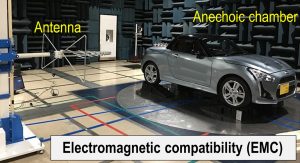
Our research team has conducted wide frequency and dynamic range EM noise measurements for the electronics to be used in an electric car (see Fig. 1). We have analysed the high possibility of EM interference with wireless mobile terminals by the radiated EM noises from a wireless power transmission (WPT) system when charging an electric vehicles (EV) battery, A receiver module compliant to cellular communication can potentially degrade wireless performance once it is located nearby the control module of WPT.
More quantitatively, the EM noise with the power of -160 dBm/Hz is observed in the frequency range of 1.7 GHz, when we measured the power at the distance of 10 cm from its surface, even in this particular example of a commercial product that perfectly satisfies EM regulations. It is therefore required to guarantee the design of IC chips and subassembly modules to be substantially considered for EMC compliance.
To solve these problems, the Secafy research team has pursued multi-layer and multi-discipline simulation techniques toward EMC awareness by design, including physical interaction of EM noise with semiconductor devices, system-level EM noise representation in a chip-package-printed circuit board (PCB) power delivery network (PDN), and system-level interaction of undesired EM radio waves with wireless communication systems. Novel materials and structures for suppressing EM noises are of other interests toward proactive remedies against EMC problems. EM measurement techniques with high fidelity, broad frequency and wide dynamic range are also essential to those developments.
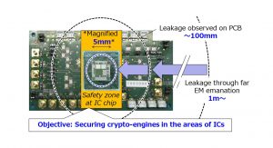
An IC chip is very tiny, typically in the size of a few millimetre square. However, the EM noise problems are widely concerned not only in ICs but also on a PCB of the size of 10 centimetres or more, as well as in a space even apart from meters typically discussed with measurements in an anechoic chamber room. If we suspect that EM noise from an IC chip carries secret information, an adversary can eavesdrop anywhere surrounding the chip (see Fig. 2). The EM side channel information leakage is one of practical threads for a secure IC chip incorporating cryptographic hardware accelerators (‘engines’).
When a cryptographic IC chip operates, power consumption current dynamically flows through PDN. This current creates the temporal change in a magnetic field nearby metallic wirings on the PDN and then emits EM radio waves and potentially leaks information handled in the background digital processing. In order to protect an IC chip from the EM side channel leakage, the Secafy research team has led to develop efficient power current simulation techniques that are leveraged by circuits and systems approach, advanced packaging and assembly technologies for suppressing EM leakage, and even on-die sensing methodologies to detect attacks by an adversary.
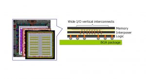
Advanced packaging boosts system performance of ESA modules and provides new possibilities of EMC capability and side channel leakage tolerance. One of extremely dense and highly functional integration can be realised with three dimensional (3D) IC chip stacking. A 3D IC demonstrator includes (see Fig. 3) memory and logic dies with active Si interposer in a single stack and packaged in a ball grid array (BGA). Continually, Si via (TSV) technology provides vertical interconnects among the memory and logic circuits with very wide bus widths.
The demonstrator exhibited the maximum data transfer rate of 100 Gbyte/sec with very low energy consumption of 0.56 pJ/bit, though the vertical bus with 4096 bits in parallel. In addition, the 3D IC chip stacking provides excellent capabilities on electrostatic discharge (ESD) protection as well as EM noise suppression. Along the aforementioned successful demonstration of 3D IC technology, the Secafy research team has been exploring a variety of advanced packaging technologies intending higher security of IC chips.
In summary, the technologies for EMC compliance of IC chips have been developed from a variety of research angles including measurements, low and high level simulation, new material adoption and advanced packaging. The research directions on hardware security widely covers the topics of cryptographic engines with high functionality and efficiency, security IC chips with their own authenticity reliably maintaining from designs to supply chains, attainments of high resiliency against the attacks of snooping mainly through side channels, and so forth, which are nevertheless very much relevant to EMC problems in IC chips.
Therefore, the deployment of EMC compliant IC chip techniques outlined here will be naturally taken in the design and development of hardware security. The Secafy research team has launched several research items for IC chips and ESAs for mission critical applications, with emphasising bilateral knowledge interaction between EMC and hardware security.
About Makoto Nagata
Makoto Nagata received a B.S. and M.S. degree in physics from Gakushuin University, Tokyo, in 1991 and 1993, respectively, and a Ph.D. in electronics engineering from Hiroshima University, Hiroshima, in 2001. He was a research associate at Hiroshima University from 1994 to 2002, an associate professor at Kobe University from 2002 to 2009 and promoted to a full professor in 2009. He is currently a professor of the graduate school of science, technology and innovation, Kobe University, Kobe, Japan. He is a senior member of IEICE and IEEE.
Dr Nagata has been a member of a variety of technical program committees of international conferences such as the Symposium on VLSI Circuits (2002-2009), Custom Integrated Circuits Conference (2007-2009), Asian Solid-State Circuits Conference (2005-2009), International Solid-State Circuits Conference (2014-2017) and many others. He is chairing the Technology Directions subcommittee for International Solid-State Circuits Conference (2018-present). He was a technical program chair (2010-2011), a symposium chair (2012-2013) and an executive committee member (2014-2015) for the Symposium on VLSI circuits. He is the past chair for IEEE Solid-State Circuits Society (SSCS) Kansai Chapter (2017-2018) and currently an AdCom member to the IEEE SSCS (2020-) and also serves as a distinguished lecturer (DL) in the society (2020-). He is an associate editor for IEEE Transactions on VLSI Systems (2015-present).
Professor Makoto Nagata
Graduate School of Science, Technology and Innovation, Kobe University
Graduate School of System Informatics, Kobe University
+81 788036569
nagata@cs.kobe-u.ac.jp
www.stin.kobe-u.ac.jp/en
Please note, this article will also appear in the first edition of our quarterly publication, the Innovation Platform.


