Researchers at Linköping University, Sweden, have developed a new molecule, indium triazenide, that can be used to create high-quality indium nitride for use in high-frequency electronics.
The bandwidth we currently use for wireless data transfer will soon be full. If we are to continue transmitting ever-increasing amounts of data, the available bandwidth must be increased by bringing further frequencies into use. Since molecules in the atmosphere adsorb electromagnetic radiation at certain frequencies, new bandwidth can only be explored at very high frequencies. To create electromagnetic signals of such high frequencies, transistors where electrons can be set in motion at those frequencies are needed. Such transistors must be made of semiconductor materials, within which it is very easy for electrons to move. Indium nitride stands out as a semiconductor material highly suited for such high frequency transistors.
“Since electrons move through indium nitride extremely easily, it is possible to send electrons backwards and forwards through the material at very high speeds and create signals with extremely high frequencies. This means that indium nitride can be used in high-frequency electronics, where it can provide, for example, new frequencies for wireless data transfer,” says Henrik Pedersen, a professor of inorganic chemistry at the Department of Physics, Chemistry and Biology at Linköping University. He has led a recent study on making very thin layers of indium nitride, which was recently published in Chemistry of Materials.

Indium nitride – CVD and ALD
Indium nitride is a chemical compound consisting of equal amounts of nitrogen and the metal indium. It is a semiconductor and can therefore be used to make transistors, the small electrical switches on which all electronic devices are based. To make a transistor, thin layers of materials with highly controlled electrical properties must be stacked on top of each other. The problem, however, is that it is difficult to produce thin films of indium nitride. Thin films of similar semiconductor materials are often produced using a well-established method known as chemical vapour deposition, or CVD, where vapours of precursor molecules containing the atoms needed for the material are allowed to react with each other and with the surface where the material is to be deposited. CVD of metal nitride semiconductors typically need temperatures between 800 and 1,000°C to activate the chemical reactions and to deposit high quality material. However, indium nitride breaks down into metallic indium and nitrogen gas when it is heated above 600°C.
The deposition chemistry in CVD has a gas phase and a surface component. The origin of the high temperatures employed in the CVD of nitrides is the slow gas phase decomposition chemistry of the ammonia molecule, which is used as the precursor molecule for nitrogen. In CVD processes, for indium nitride this has been compensated by a very high surplus of ammonia. The researchers at Linköping University speculated that if the surface chemical reactions between ammonia molecules and chemisorbed indium precursor molecules could be enhanced by a monolayer of indium precursors and stabilised by lower temperature, then the overall process temperature could be reduced. They therefore started experimenting with time-resolved CVD processes for indium nitride.
The researchers eventually started using the most well-known time-resolved form of CVD, known as ‘atomic layer deposition’, or ALD. ALD is an essential technique for all modern electronics fabrication and relies on sequential supplies of the precursor molecules, meaning that the precursor molecules for indium and nitrogen cannot react with each other here (as they do not meet in the gas phase), while they can on the surface as this is saturated with the opposite precursor molecules. ALD is also done at lower temperatures than traditional CVD, meaning that ALD is a very interesting option for indium nitride. The researchers hypothesised that the surface chemical reactions governing ALD will help the indium nitride films to grow at lower temperatures without lowering the material quality. While ALD of indium nitride has been shown before, the low temperature in ALD meant that large amounts of carbon, emanating from the indium precursor molecule, was trapped in the indium nitride film.
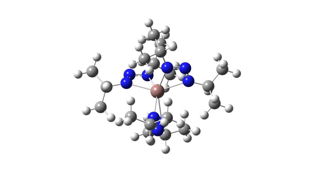
Indium triazenide
The researchers started exploring alternative precursor molecules for indium where the indium-carbon bonds in the traditional indium precursor are replaced by weaker indium–nitrogen bonds. Three such molecules had been reported in the scientific literature, all with indium-nitrogen bonds formed by six nitrogen atoms binding to one indium atom. The nitrogen atoms form pairs bridged by a carbon atom. The researchers tried all of them and discovered that the fewer atoms attached to that central carbon atom, the better quality on the deposited indium nitride. The best quality was obtained when a single hydrogen atom was bonded to the carbon.1
From this result, the scientists developed a new precursor molecule for indium, where the atomic bridge between the nitrogen atoms is replaced by a third nitrogen atom. This sort of molecule with three nitrogen atoms in a row is called a ‘triazenide’. Since nitrogen forms one less bond than carbon, no further atoms are needed to complete the bridge and the molecule thus became even smaller. No one had worked with such indium triazenides previously, and the researchers soon discovered that the triazenide molecule is an excellent starting material for the manufacture of indium nitride thin films.

Materials used in electronics must, typically, be produced by allowing the thin film to grow on a surface that controls the crystal structure of the electronic material. The process is known as epitaxial growth. The researchers discovered that it is possible to achieve epitaxial growth of indium nitride if silicon carbide is used as substrate, something that was not previously known. This is very interesting since silicon carbide is a highly suited material to use as the basis for high frequency electronics since it is a very good thermal conductor and can therefore dissipate excess heat generated when creating the high frequency signals. Furthermore, the indium nitride produced in the ALD process using the new indium triazenide molecule is very pure, and among the highest quality indium nitride reported in the world.
“The indium triazenide molecule that we have invented in combination with the ALD process that we have developed, makes it possible to seriously start thinking about using indium nitride in electronic devices. We have shown that it is possible to produce indium nitride in a manner that ensures that it is sufficiently pure to be described as a true electronic material,” Pedersen said.
The researchers discovered another surprising fact – it is generally accepted amongst those who use ALD that the precursor molecules should not be allowed to react or be broken down in any way in the gas phase. But when the researchers increased the temperature in the ALD process, they discovered that there is not just one, but two, temperature intervals at which the process was stable.2
Pedersen said: “We believe that the indium triazenide breaks down into a smaller indium alkyl amine in the gas phase, and this improves the ALD process since this molecule is smaller and occupies a smaller area on the surface. The indium alkyl amine cannot be used directly as it polymerises upon heating and can therefore not be heated to form the vapour needed for the ALD process. Using molecules that are not fully stable in the gas phase is a paradigm shift within ALD. We have shown that it is possible obtain a better indium nitride thin film if we allow the indium triazenide molecule to break down to a certain extent in the gas phase.”
The researchers have worked on the closely related semiconductor material gallium nitride, which is the basis for all blue light emitting diodes to develop a gallium triazenide precursor and a corresponding ALD process for gallium nitride. The continued research will focus on gathering experimental evidence for the suggested decomposition mechanism of the triazeinde molecules in the ALD reactor. The researchers are also examining similar triazenide molecules with metals other than indium and gallium for new ALD precursors. The researchers have found that several of the other metal triazenides also show promising properties, such as volatility, for use in ALD.
The study has been carried out together with researchers from the Swedish University of Agricultural Sciences in Uppsala and Carleton University in Ottawa, Canada. It has received financial support from the Swedish Foundation for Strategic Research (SSF) and the Knut and Alice Wallenberg Foundation.

Atomic layer deposition (ALD)
The thin film of indium nitride is produced in a vacuum chamber by introducing vapours of a precursor molecule that contains indium into the chamber and allowing it to react with the surface on which the thin film is to form. This is followed by the introduction of a gas that contains nitrogen and that reacts with the surface to form a monolayer of indium nitride. By alternating between the two gases several hundred times, layers are added onto layers until the thin film is complete. Using this method, in combination with plasma discharges to make more reactive fragments of the nitrogen containing gas, the chemical reactions can take place at 300°C, which is much lower than the temperatures required during CVD, which can lie between 800 and 1,000°C.
References
- The Endocyclic Carbon Substituent of Guanidinate and Amidinate Precursors Controlling Atomic Layer Deposition of InN Films, Polla Rouf, Nathan J. O’Brien, Karl Rönnby, Rouzbeh Samii, Ivan G. Ivanov, Lars Ojamäe and Henrik Pedersen, Journal of Physical Chemistry C, published on 26 September 2019, doi: 10.1021/acs.jpcc.9b07005. Link: https://pubs.acs.org/doi/10.1021/acs.jpcc.9b07005
- ‘In Situ Activation of an Indium(III) Triazenide Precursor for Epitaxial Growth of Indium Nitride by Atomic Layer Deposition’, Nathan J. O’Brien, Polla Rouf, Rouzbeh Samii, Karl Rönnby, Sydney C. Buttera, Chih-Wei Hsu, Ivan G. Ivanov, Vadim Kessler, Lars Ojamäe and Henrik Pedersen, Chemistry of Materials, published as an open access article on 24 April, doi: 10.1021/acs.chemmater.9b05171. Link: https://dx.doi.org/10.1021/acs.chemmater.9b05171
Henrik Pedersen
Professor
Department of Physics, Chemistry and Biology (IFM)
Linköping University
+46 13 281385
henrik.pedersen@liu.se
Tweet @hacp81
https://liu.se/en/research/pedersen-group
Please note, this article will also appear in the third edition of our new quarterly publication.