
The NanoEngineering Network explains how Smart Metasurface Technology (a class of metamaterials) and the related concept of ‘omniconnectivity’ has the potential to boost Europe’s competitiveness in the field of electronics
‘Metamaterials’ refers to the artificial arrangement of multiple elements, carefully engineered to achieve advantageous and unusual electromagnetic or optical properties not present in Nature. It is a growing field that is now recognised all over the world. For example, ‘optical metalenses’ have been considered in the Top Ten Emerging Technologies by the World Economic Forum in 2019. During Horizon 2020, more than 60 projects (>20 ERC grants) based on metamaterials have been funded. Furthermore, metamaterials have been identified as a valuable path for exploitation, even beyond civil applications.
An important class of metamaterial are ‘metasurfaces’, thin versions of metamaterials, which artificially modify the boundary conditions more than the constitutive parameters of the material. Furthermore, thanks to different actuation mechanisms (electrostatic, magnetostatic, thermal, optical, etc.) reconfigurability becomes possible.
If we now imagine including distributed sensors and actuators to those active metasurfaces with exotic electromagnetic properties, we can create a novel key-enabling non-invasive broadband technology, which we denote here as ‘Smart Metasurface Technology’ (SMT). Preliminary documents in the next Horizon Europe calls already refer to this technology as ‘Smart Skin’.
Such technology opens the path for a new era in communication and interaction between people, machines, and their environment. SMT puts humans and their interactions at the centre of the future digital society. This concept, which we call ‘omniconnectivity’, will be further elaborated on in the next section. It relies upon the mastery of nano-engineering across a wide range of scales and frequencies. Europe and European industries will have a chance to acquire worldwide leadership for the new generation of ICT nanosystems, with an enormous impact on the economy. It will also be a major contribution to the current and forthcoming discussions beyond Moore’s Law and it will contribute to the repositioning of Europe in the ICT domain, beyond 5G.
Of course, this visionary approach can only be reached through a very large-scale effort, considerably transcending the scope and extent of any conventional collaborative project. That is why a large initiative has been launched, incorporating selected institutions from the community of nanoarchitectronics, metamaterials, spintronics, photonics, and phononics. This initiative has been proposed and well ranked in the last call for EU Flagships, which unfortunately was finally aborted.
Today, even more due to the context of the COVID-19 pandemic, our approach represents an opportunity to strengthen the position of Europe worldwide, fostering a true Renaissance of EU-based ICT platforms and a new way of defining and exchanging data. Our initiative should be considered as a Dedicated Mission in the Horizon Europe framework, as overall knowledge is definitely settled in Europe.
Omniconnectivity
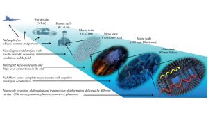
Omniconnectivity encompasses real-time communication, sensing, monitoring, and data processing among humans, objects, and their environment (see Fig. 1). The omniconnectivity vision encompasses people in a new sphere of extremely simplified, intuitive, and natural communication. All ICT users could benefit from this new experience and see their quality of life enhanced in their everyday living and practice.
A key enabling technology
The key enabling technology is denoted ‘Smart Metasurface Technology’ (SMT), and is based on smart metasurfaces (SM) – non-invasive, wireless, ultraflat functional systems which communicate with each other by exploiting networks (from the local up to the satellite level) and by using the whole frequency spectrum from microwave frequency to optics (see Fig. 1). SMT will be applicable to any surface, on any physical item, and thereby exponentially diversifies and increases connections among humans, wearables, vehicles, and everyday objects.
SMs will be a highly complex hierarchical bidirectional (transmitting/receiving) system, extremely thin at human scale, but complex at nanoscale (see Fig. 2). SMT will integrate enhanced connection/elaboration capabilities and sensor functionalities at different scales (nano-, micro-, meso-, macro-scale). It will be intrinsically secure by material construction, energetically self-sufficient due to ad-hoc energy harvesting integrated modules, and cognitive/adaptive via environment awareness. Its size at human scale will depend on the operational frequency range: it may have a size of up to several centimetres for an individual SM, and unlimited virtual dimensions when connected to co-operative SM networks.
The creation of the SMT is the centrepiece and unifying scientific and technological goal of our action. Its creation requires an extraordinary and long-term effort in the integration of heterogeneous materials through nano-fabrication and multiscale modelling/design. In the long term, SMTs will boost omniconnectivity by reducing the interaction with hand-held ICT to a minimum and, finally, making it ‘transparent’ to the user. SM will be composed of nano-objects, forming elementary functional items, which are aggregated/integrated in different shapes and scales (from sub-nanometre to human-eye scale) to form systems whose final visible scale can have different dimensions, depending on the specific application and operational frequency range.
To successfully operate across the whole range of frequencies and functionalities, SM will have a number of features, including:
- Transmit/receive: it will be able to transmit/receive electromagnetic (EM) waves to communicate with other devices and other SMs;
- Transparent: non-invasive in the mid-term (before 2030) and eventually inconspicuous in the long-term (before 2040), with seamless integration into surface structures of everyday objects;
- Interoperable with the user: capable to seamlessly perceive a stimulus from a user, make a decision, and make a consequent action or response;
- Reconfigurable: it will be able to change configuration in ultra-fast (below ns) timescale;
- Multifrequency: it will be able to cover a wide range of frequencies for different connectivity purposes;
- Upscalable: covering large scale surfaces by wave interaction with other SM and by cloud-communication;
- Adaptive: it will be able to adapt spontaneously to changes in the environment;
- Smart: it will be able to perform simple computation tasks and massive computation in co-operation with other SMs or through communication with the Cloud;
- Cognitive: it will be able to learn from its environment by collecting information from other SMs;
- Secured: it will be protected against tampering, hacking or other digital aggression; and
- Efficient: it will enable extremely low loss and ultra-low power consumption as well as full autonomy in the long-term.
Today, this may sound impossible, however recent breakthroughs in nanoengineering show the way to make it real.
Fundamental Scientific approach
SMT will exploit EM waves for transmitting/ receiving information to/from the environment and will use heterogeneous wave-type physical mechanisms to transfer the information between different points of the nano-structured material. The EM wave transmission/reception functionality will be performed, depending on the frequency, by the dynamic reconfigurability and adaptation of the EM boundary conditions at the interface with the free-space, or by creating a virtual effective sensitive surface through communication with other SMs.
In reception mode, the SM reconfigurability will be performed adaptively in order to maximise the coupled energy on a large scale of frequencies, matching the boundary with the spatial change of the external EM signal. The transfer of information between different points of the SM at nanoscale distances will exploit the emerging electromagnetic properties of nanomaterials and their interaction with photons and other quasi-particles (spins, magnons, phonons, etc.) as information carriers to make the SM cognitive. The ground-breaking unifying approach is the use of all wave phenomena almost in their entirety, deploying the state variables best suited for any given information-processing task at component, system, and network level.
The SMT revolution of communication
SM and computing resources integrated on the surface of any infrastructure, transportation platform, or everyday object will interact upon request, activated by an SM belonging to a person. A simple touch, a near field interaction, and/or a wireless transmission will allow the transfer of pre-determined information from and to a network of sensors and devices. These will trigger reactions/actions that could prevent accidents, adapt the living/working environment at predefined personal settings, or take preventative measures in the case of health issues. If a more structured interaction with an instrument/device is required, SMT-driven holographic interfaces (e.g., a holographic keyboard) will be used to interact with other communication devices, or with any complex instruments physically located or integrated at other places. This will open a new era of truly intuitive, hands-free, human-machine collaboration, while reserving the relevant decisions about interactions to the human in a fully secured and personal sphere (see SMT and data protection in next section).
Transparency
Transparent technology refers to a non-invasive technology which makes use of minimum number of devices and which is minimally visible to the user. The technology will become increasingly ‘unnoticeable’ and simple to use, while remaining pervasive, and will also remain totally secure and controllable by the user. In the future, it will no longer be necessary to use keyboards, smart phones, PCs, or smart watches. Through touching/sensing or using voice commands, the SMT will allow users to become connected or to enable/disable functions. It will shift the paradigm of communication from symbolic and textual to gestural, haptic, and verbal modalities (the ‘Tactile Internet’).
SMT will allow system-control upon perceptual motion skills, relying on the way humans physically interact with their environment. It will support interaction with computation through our full human and bodily capabilities such as walking, touching, and cueing.

The integration of functionalities
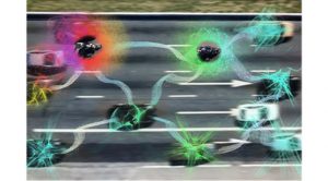
The proposed technology allows a huge number of micro- and nano-devices to be integrated onto a single interface, thereby providing an unprecedented number of coexistent functionalities. Sensing and actuation will be integrated into a single SMT, leading to extraordinary developments in haptics and smart material actuators. Furthermore, a network of SMTs will permit sensing information and action commands to be despatched in an efficient and natural way. The fusion of this amount of sensing information will anticipate and prevent possible dangerous situations, operating in the background, (e.g. the lack of a driver’s responsiveness) or to identify global risks, such as urban pollution, or imminent calamities, providing a capillary and almost instantaneous network of information and the initiation of required preventive actions.
Computations and cognitions
Thanks to the extreme reconfigurability of the SMT network, new computation models (e.g. neuromorphic schemes) can also be implemented, choosing the most suitable solution for a given computation task. Simple computation tasks can be performed by single SM and more complex tasks by SM networks or remotely by Clouds. Furthermore, SMs can be connected to distributed computational networks performing a specific task in time by developing ad hoc cognitive capabilities through mutual dynamic reconfiguration.
Data Protection
The striking potential of SMT is further enhanced by its ability to ensure both top security and personal privacy control. Due to the intrinsic nature of SMT, secure functions will be implemented naturally and used for real-time data cryptography. Operating at the nanoscale will benefit from the quantum properties and thus create robust hardware modules such as encryption/decryption key generators with a high degree of randomness (e.g., spin- or photonic-based random generators). Furthermore, the embedded computation capability will further enhance this module security by pre-processing on local nodes before connection with the external environment (edge computing).
Autonomy
Energy harvesting modules based on spintronics and other novel technologies will enable SMs to harvest energy directly from their environment. The power consumption of ICT, including local or remote computation, will be reduced to the very minimum to reach 24/7 autonomy in the long term. SMs will be automatically recharged by a certain movement or by the body heat of an individual. SMs applied to objects, such as cars or satellites, will be recharged by the actuation of breaks or by the surrounding electromagnetic radiation.
Conclusions
To conclude, we believe that Smart Metasurface Technology, and the related concept of omniconnectivity, is a great opportunity for Europe to reinforce its position on the market of communication and electronics compared to other macro-regions (such as the USA and China and the rest of Asia). It will provide EU companies, from SMEs to large groups, from those which already exist to new spin-offs and start-ups, with a new opportunity to have a stronger role in the development of the future of electronics, a sector which has been overwhelmed by the concentration of silicon foundries in Asia. These are all examples of a clear benefit which will increase the competitiveness of EU industry and the influence of EU companies in specific market segments. This will bring back investments, high value-added industries, and growth to the EU.
It is high time the European Commission considers this initiative as a Dedicated Mission in the Horizon Europe framework, paving the way for the Renaissance of EU-based ICT.
Other participants from the NanoEngineering network:
Stefano MACI (Università di Siena); Giampiero GERINI (TNO); Jean CHAZELAS (Ultimetas); Daniel DOLFI (Thales); Thi-Quynh-Van HOANG (Thales); Brigitte LOISEAUX (Thales); Alessandro GARIBBO (Leonardo); Giuseppe VECCHI (Politecnico di Torino); Filiberto BILOTTI (Università Roma 3); Charlotte TRIPON-CANSELIET (ESPCI PARIS)
Paolo Bortolotti
Director
Joint laboratory CNRS-Thales at Palaiseau
Director
SpinTronicFactory
paolo.bortolotti@thalesgroup.com
https://cnrs-thales.fr
www.spintronicfactory.eu
Please note, this article will also appear in the fourth edition of our new quarterly publication.


